Refresh control circuit, semiconductor memory device, and refresh method thereof

a control circuit and memory device technology, applied in the field of semiconductor memory devices and refresh control circuits, can solve the problems of leaking or discharged charges from the cell capacitor, affecting the operation of the cell capacitor, and changing the charge stored in the cell capacitor,

Active Publication Date: 2019-09-12
SK HYNIX INC
View PDF4 Cites 54 Cited by
  • Summary
  • Abstract
  • Description
  • Claims
  • Application Information

AI Technical Summary

Problems solved by technology

However, in reality, the charges stored in the cell capacitor may change due to a voltage difference between the voltage of the capacitor and the voltage of a peripheral circuit.
As a result, stored charges may be gradually leaked or discharged from the cell capacitor.
Also, when the cell capacitor is in a discharged state, some charges may be leaked from the cell capacitor.
These changes in the charges stored in the cell capacitor means that the data stored in the cell capacitor may be lost.
However, a refresh operation may significantly increase the operational load of a memory device.

Method used


Image

  • Refresh control circuit, semiconductor memory device, and refresh method thereof
  • Refresh control circuit, semiconductor memory device, and refresh method thereof
  • Refresh control circuit, semiconductor memory device, and refresh method thereof

Examples


Embodiment Construction

[0019]Exemplary embodiments of the present invention will be described below in more detail with reference to the accompanying drawings. The present invention may, however, be embodied in different forms and should not be construed as limited to the embodiments set forth herein. Rather, these embodiments are provided so that this disclosure will be thorough and complete, and will fully convey the scope of the present invention to those skilled in the art. Throughout the disclosure, like reference numerals refer to like parts throughout the various figures and embodiments of the present invention.

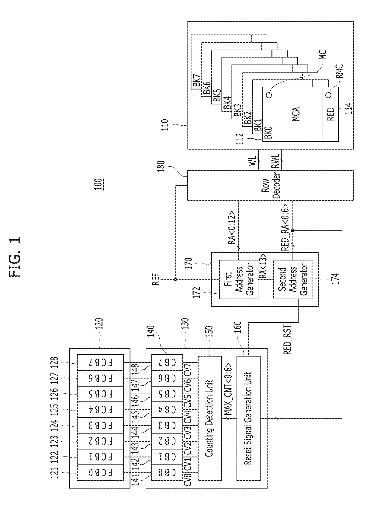
[0020]As semiconductor fabrication technology advances, the degree of integration of semiconductor memory devices is gradually increasing, and the number of cells to be subjected to a refresh operation is also increasing. To reduce the time required for the refresh operation, a method of simultaneously performing a one-time refresh operation onto a plurality of cells is proposed. For example...


PUM


Abstract

A semiconductor memory device includes: first to Nth memory banks each including a normal cell region coupled to normal word lines and a redundant cell region coupled to redundant word lines; first to Nth non-volatile memories that correspond to the first to Nth memory banks, respectively, each including a plurality of memory sets for programming repair addresses of the corresponding memory banks; a refresh control circuit for generating first to Nth count values by counting a number of the memory sets used in the first to Nth non-volatile memories, and generating a redundant reset signal based on the first to Nth count values; and an address generation circuit for sequentially generating normal addresses for selecting the normal word lines and redundant addresses for selecting the redundant word lines based on a refresh signal, and initializing the redundant addresses based on the redundant reset signal.

Description

CROSS-REFERENCE TO RELATED APPLICATIONS[0001]The present application claims priority under 35 U.S.C. § 119(a) to Korean Patent Application No. 10-2018-0026946, filed on Mar. 7, 2018, which is incorporated herein by reference in its entirety.BACKGROUND1. Field[0002]Exemplary embodiments of the present invention relate to a semiconductor technology, and more particularly, to a semiconductor memory device that performs a refresh operation.2. Description of the Related Art[0003]Generally, a semiconductor memory device may include a plurality of memory banks for storing data. Each of the memory banks may include tens of millions of memory cells including a cell capacitor and a cell transistor. The semiconductor memory device may store data by charging or discharging the cell capacitor.[0004]Ideally, the charges stored in the cell capacitor should remain constant if there is no control applied. However, in reality, the charges stored in the cell capacitor may change due to a voltage diffe...

Claims


Application Information

Patent Timeline
Patent Type & Authority Applications(United States)
IPC IPC(8): G11C11/406G11C29/00G11C11/408G11C11/4072
CPCG11C29/787G11C29/783G11C11/4085G11C11/40618G11C11/4072G11C29/76
Inventor KIM, DO-HONG
Owner SK HYNIX INC
Why Eureka
Try Eureka