

Reference voltage generation circuit
- Summary
- Abstract
- Description
- Claims
- Application Information
AI Technical Summary
Benefits of technology
Problems solved by technology
Method used
Image

Examples
first embodiment
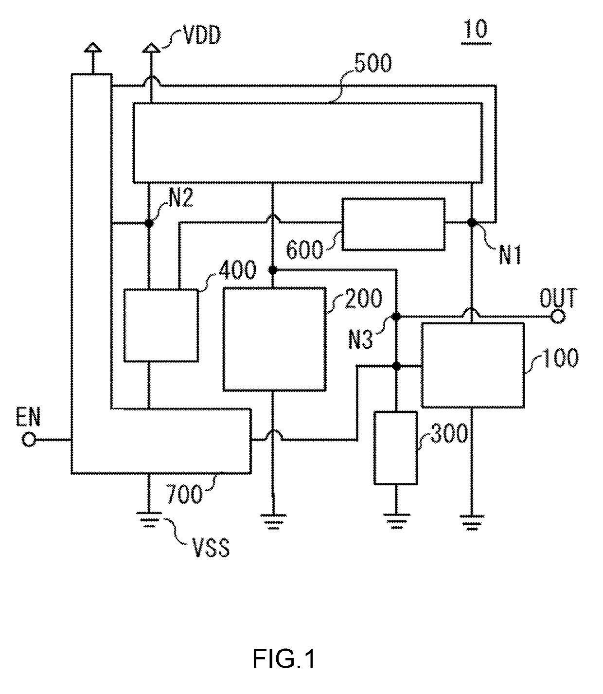
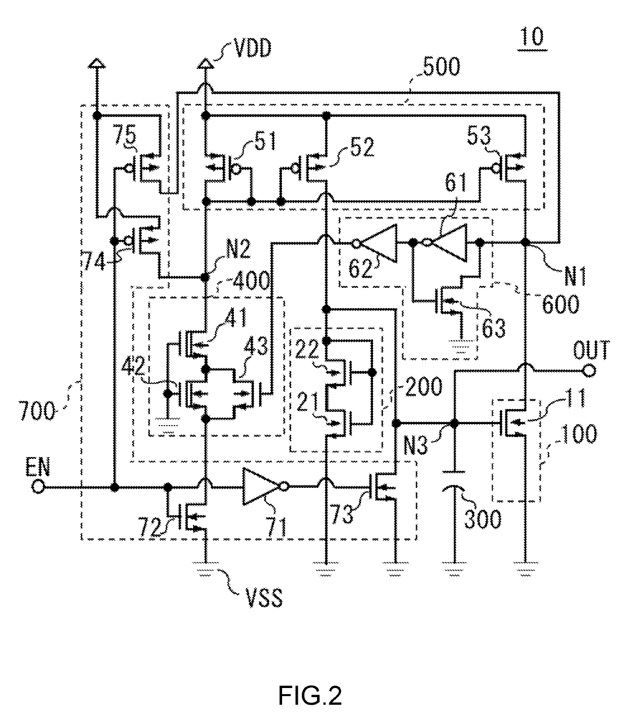
[0019]FIG. 1 is a block diagram for illustrating the configuration of a reference voltage generation circuit 10 according to a first embodiment of the present invention. The reference voltage generation circuit 10 includes an input terminal EN, an output terminal OUT, a voltage detection circuit 100, a reference voltage circuit 200, a stabilizing capacitor 300, a current source circuit 400, a current mirror circuit 500, a latch circuit 600, and a control circuit 700. The reference voltage generation circuit 10 switches between a non-operation state and a normal operation state if a control signal enters to the input terminal EN.
[0020]The input terminal EN is connected to the control circuit 700. The control circuit 700 is connected via a node N1 to the voltage detection circuit 100, the current mirror circuit 500, and the latch circuit 600, connected via a node N2 to the current source circuit 400 and the current mirror circuit 500, and connected via a node N3 to the output terminal...
second embodiment
[0035]FIG. 4 illustrates a reference voltage circuit 200a and voltage detection circuit 100a in a reference voltage generation circuit (which will be hereinafter referred to as “second reference voltage generation circuit”) according to the second embodiment of the present invention. The second reference voltage generation circuit has the same components as in the reference voltage generation circuit 10 (illustrated in FIG. 2) except the voltage detection circuit 100 (illustrated in FIG. 2) and the reference voltage circuit 200 (illustrated in FIG. 2). The reference voltage circuit 200a is obtained by replacing the transistors of the reference voltage circuit 200 with a three-stage cascode connection circuit that is made up of the enhancement NMOS transistors 21 and 22 and an enhancement NMOS transistor 23, and the voltage detection circuit 100a is obtained by replacing the transistor of the voltage detection circuit 100 (illustrated in FIG. 2) with a two-stage cascode connection ci...
third embodiment
[0039]FIG. 5 illustrates a current source circuit 400a in a reference voltage generation circuit (which will be hereinafter referred to as “third reference voltage generation circuit”) according to the third embodiment of the present invention. The third reference voltage generation circuit has the same components as in the reference voltage generation circuit 10 (illustrated in FIG. 2) except the voltage detection circuit 400 (illustrated in FIG. 2). The current source circuit 400a is obtained by replacing the depletion NMOS transistors 41 and 42 of the current source circuit 400 in the reference voltage generation circuit 10 with depletion PMOS transistors 44 and 45, and connecting gates of the PMOS transistors 44 and 45 to the node N2 (illustrated in FIG. 2). The operation of the reference voltage generation circuit is the same as the operation of the reference voltage circuit 10, and a description on the operation is therefore omitted.
PUM
 Abstract
Description
Claims
Application Information