Non-destructive in-situ elemental profiling

Inactive Publication Date: 2006-10-12
GOOGLE LLC
View PDF16 Cites 0 Cited by
  • Summary
  • Abstract
  • Description
  • Claims
  • Application Information

AI Technical Summary

Benefits of technology

[0009] The invention includes a non-destructive in-situ elemental profiling of a layer in a set of layers method and system. In one embodiment, a first emission of a plurality of photoelectrons is caused from the layer to be elementally profiled. An elemental profile of the layer is determined based on the emission. In another embodiment, a second emission of a plurality of photoelectrons is also received from the layer, and an elem

Problems solved by technology

Unfortunately, removal of a product from the manufacturing environment creates a number of disadvantages.
First, any removal of a product from the manufacturing process increases processing time.
Second, it prohibits “on-the-fly” adjustments to process conditions, e.g., gas flow rates, annealing temperature, pressure, etc.
Third, c

Method used


Image

  • Non-destructive in-situ elemental profiling
  • Non-destructive in-situ elemental profiling

Examples


Example

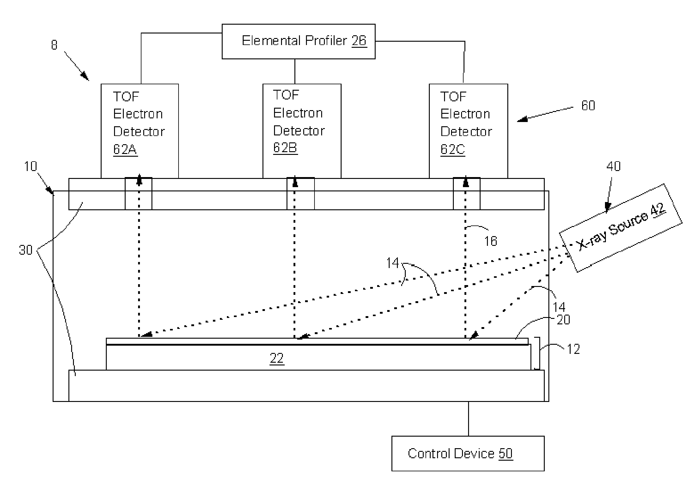
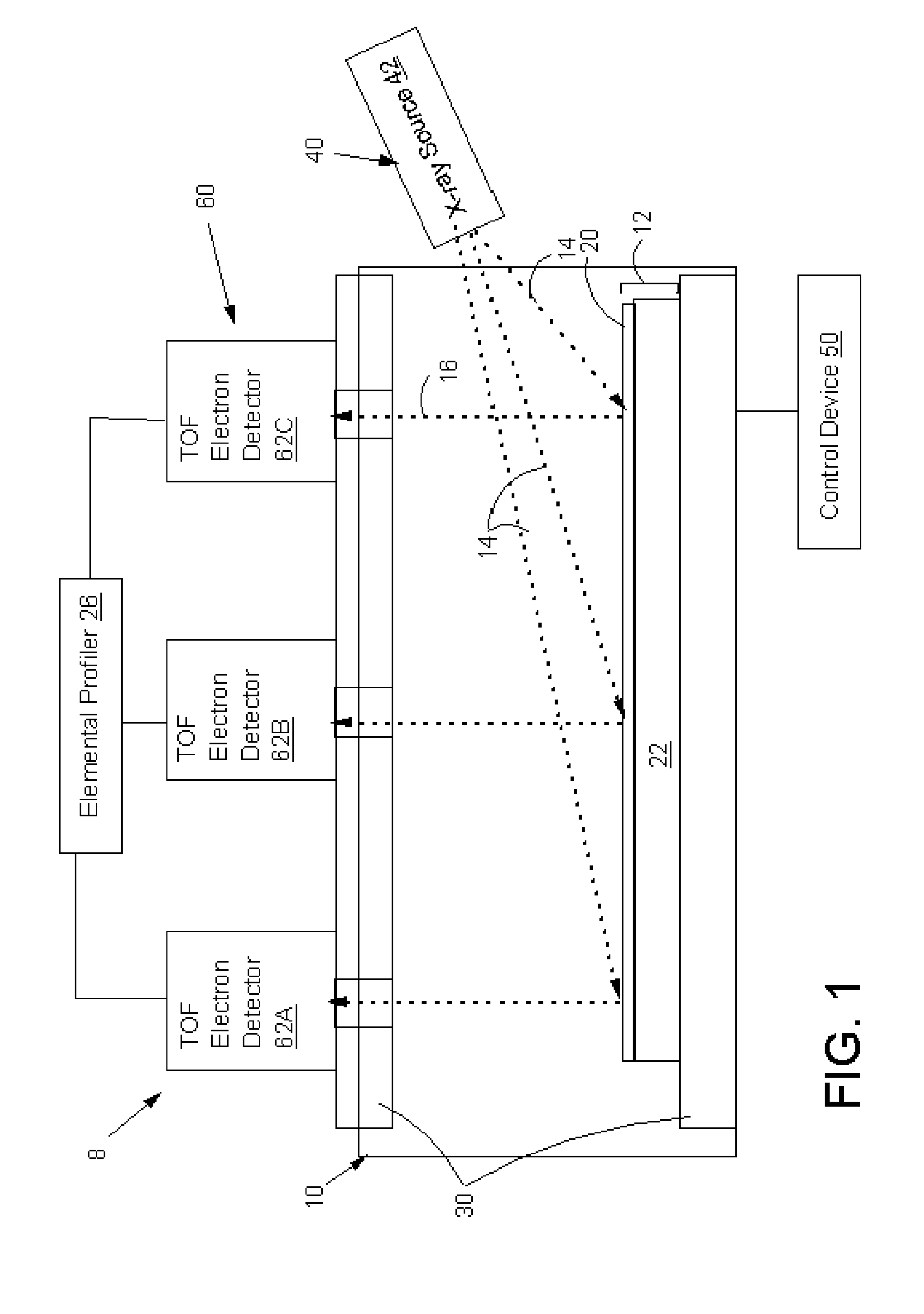
[0016] With reference to the accompanying drawing, FIG. 1 illustrates an elemental profiling system 8 according to the invention. As shown in FIG. 1, the invention determines an elemental profile, e.g., of a composition, of a layer in a set of layers undergoing a process in situ of a process chamber 10. In accordance with the invention, a layered material 12 including a topmost layer 20, e.g., a semiconductor, dielectric, or conductor of a semiconductor wafer, is irradiated with an x-ray beam 14, which comprises a plurality of photons, and a photoelectron emission 16 is caused in response to this irradiation. Photoelectron emissions 16 have signals with energy levels unique to the material of layer 20 from which the photoelectrons are emitted. The material can be a compound or an element, but the material of layer 20 and a set of layers (layered material 12) thereabout (under, adjacent or over) differ only in stoichiometry. Because photoelectrons have a short mean free path, photoel...


PUM


Abstract

A non-destructive in-situ elemental profiling of a layer in a set of layers method and system are disclosed. In one embodiment, a first emission of a plurality of photoelectrons is caused from the layer to be elementally profiled. An elemental profile of the layer is determined based on the emission. In another embodiment, a second emission of a plurality of photoelectrons is also received from the layer, and an elemental profile is determined by comparison of the resulting signals. A process that is altering the layer can then be controlled “on-the-fly” to obtain a desired material composition. Since the method can be employed in-situ and is non-destructive, it reduces turn around time and lowers wafer consumption. The invention also records the composition of all processed wafers, hence, removing the conventional statistical sampling problem.

Description

[0001] This application is related to co-pending U.S. Ser. No. 10 / 904,883, entitled “Endpoint Detection for the Patterning of Layered Materials,” filed Dec. 2, 2004, which is hereby incorporated by reference.BACKGROUND OF THE INVENTION [0002] 1. Technical Field [0003] The present invention relates generally to composition determination techniques, and more particularly, to non-destructive, in-situ elemental profiling. [0004] 2. Related Art [0005] Conventionally, determination of a composition or elemental profiling of a film, for example, in the semiconductor industry, requires testing in a location out of the manufacturing environment. Unfortunately, removal of a product from the manufacturing environment creates a number of disadvantages. First, any removal of a product from the manufacturing process increases processing time. Second, it prohibits “on-the-fly” adjustments to process conditions, e.g., gas flow rates, annealing temperature, pressure, etc. Third, conventional testing...

Claims


Application Information

Patent Timeline
IPC IPC(8): G01J3/40
CPCG01N23/2273
Inventor PANDA, SIDDHARTHASIEVERS, MICHAEL R.WISE, RICHARD S.
Owner GOOGLE LLC
Why Eureka
Try Eureka