

Thermoelectric conversion module
- Summary
- Abstract
- Description
- Claims
- Application Information
AI Technical Summary
Benefits of technology
Problems solved by technology
Method used
Image

Examples
Example
Working Examples and Comparative Examples
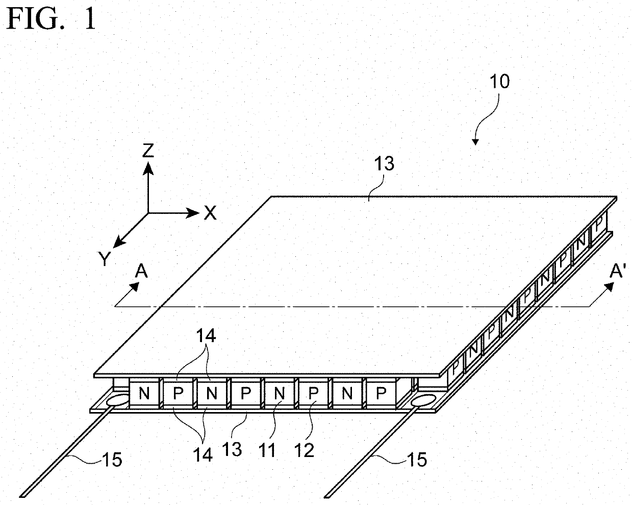
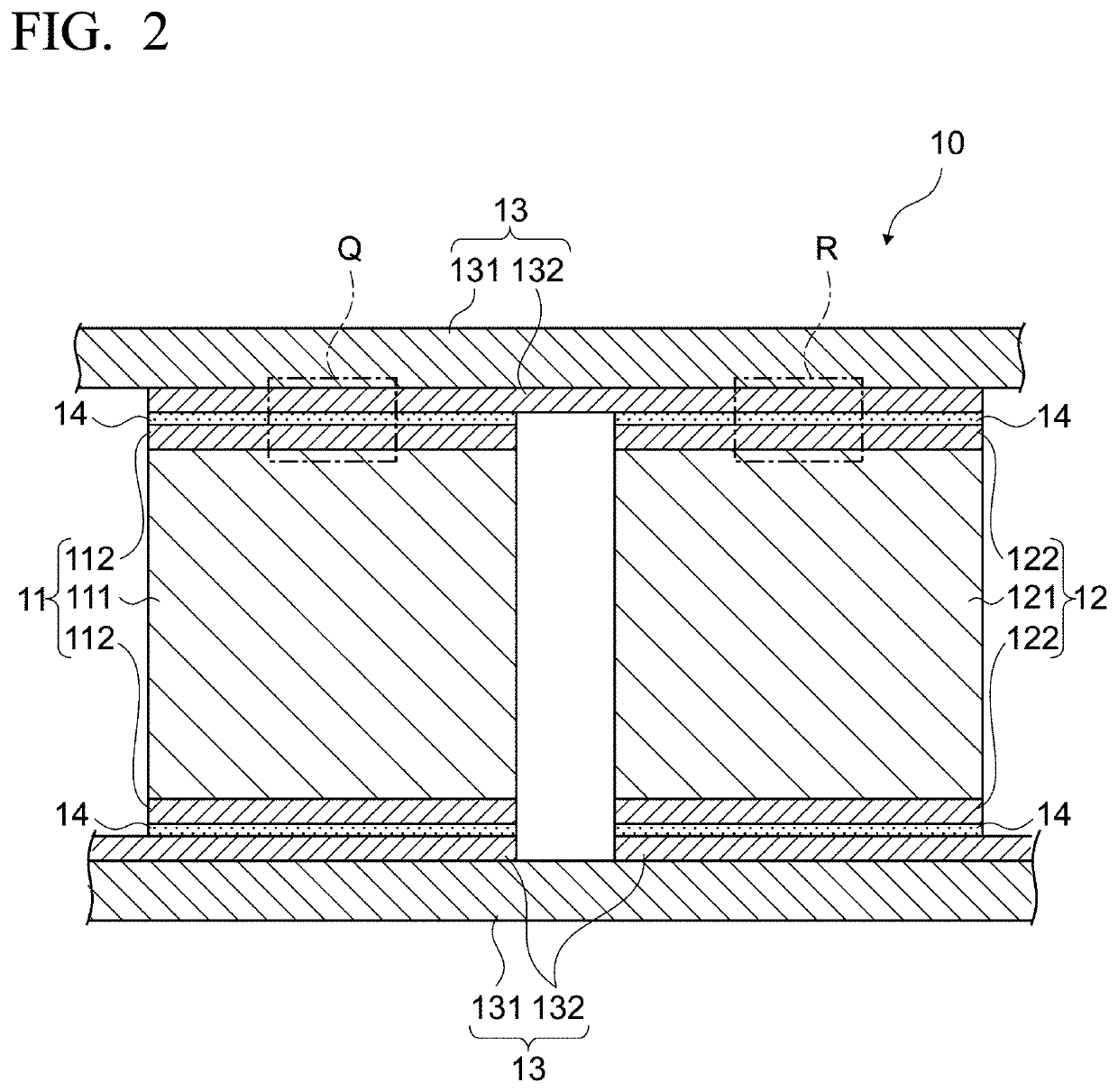
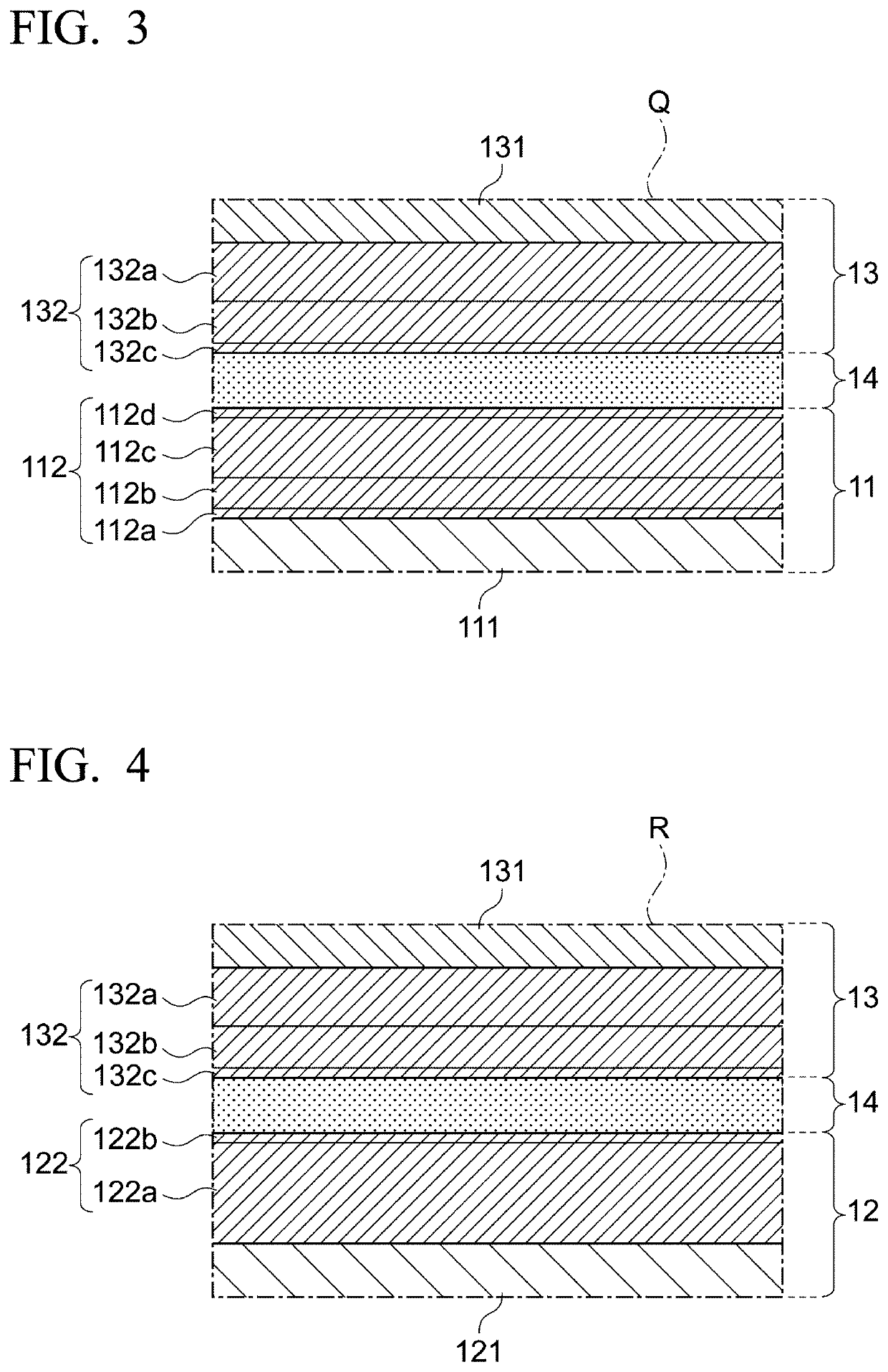
[0063]Hereinafter, working examples as examples of the configuration of the above-described embodiment, and comparative examples as examples of a configuration different from the above-described embodiment will be explained. However, the present invention is not limited to configurations of the working examples described below. Specifically, in the working examples and the comparative examples, the effect of the aluminum layer 112b and effects of the aluminum layer 112b and the nickel layer 112c were observed.
(Effect of Aluminum Layer 112b)
[0064]In order to confirm the effect of the aluminum layer 112b as the diffusion prevention layer for nickel in the first electrode 112 of the N-type chip 11, a sample of an N-type chip according to a comparative example in which the aluminum layer 112b was not provided was prepared.
[0065]Since the aluminum layer 112b was not provided in the sample of the N-type chip according to the comparative example, th...
Example
[0073]Specifically, in the sample of the N-type chip according to the comparative example 1, the thickness of the nickel layer 112c was set to 4 μm. In the sample according to the comparative example 2, the thickness of the nickel layer 112c was set to 10 μm. Therefore, the sample according to the comparative example 2 has a configuration in which the silver constituting the bonding layer 14 is less likely to diffuse into the N-type element 111 than that in the sample according to the comparative example 1.
[0074]Also, in the sample of the N-type chip 11 according to the working example, the thickness of the nickel layer 112c was set to 10 μm. Therefore, the sample according to the working example has a configuration in which the silver constituting the bonding layer 14 does not easily diffuse to the N-type element 111 as in the sample according to the comparative example 2. Further, in the sample according to the working example, a thickness of the aluminum layer 112b was set to 4 μ...
Example
[0078]Next, the comparative example 2 and the working example in which thicknesses of the nickel layers 112c are equal to each other are compared. The change rate ΔR increases with the elapse of time in the sample according to the comparative example 2 in which the aluminum layer 112b is not provided. By contrast, almost no temporal change in the change rate ΔR is found in the sample according to the working example in which the aluminum layer 112b is provided.
[0079]In the sample according to the comparative example 2, it is thought that the electrical resistance increased by progress of diffusion of the nickel constituting the nickel layer 112c into the N-type element 111 with passage of time. In contrast, in the sample according to the working example, it is thought that diffusion of the nickel into the N-type element 111 was prevented by the aluminum layer 112b.
Other Embodiments
[0080]Although the embodiments of the present invention have been described above, the present inventi...
PUM
 Abstract
Description
Claims
Application Information