Method of making solar cell

a manufacturing method and solar cell technology, applied in the field of manufacturing a solar cell, can solve the problems of affecting the supply of silicon wafers, consuming a lot of time for described periphery processing with respect to each of the silicon wafers, and affecting the quality of the solar cell, so as to achieve the effect of surface roughness of the side faces

Inactive Publication Date: 2009-12-29
SHARP KK
View PDF22 Cites 3 Cited by
  • Summary
  • Abstract
  • Description
  • Claims
  • Application Information

AI Technical Summary

Benefits of technology

[0047]The silicon block 1 of 125×125×250 mm obtained in Example 1 was polished by Method 1 to confirm the effect of the invention. A sponge wheel and a mixture of GC abrasive grains (#800) with polish oil were used as the polishing member 13 and the slurry 8, respectively.
[0048]As a result, four side faces 9 were polished in 16 minutes. Surface roughness Ry of the side faces was reduced from 20 μm to 5.8 μm by the polishing.Example 3Method 1, Using Resin Brush

Problems solved by technology

However, flattening of the fine surface roughness existing on its side faces has not been conducted.
Since the solar cell requires a large number of silicon wafers as compared with IC and LSI, the above-described periphery processing with respect to each of the silicon wafers consumes a lot of time, investment in equipment and labor.
This may delay the supply of the silicon wafers behind the demand.
Further, the etching requires equipment for liquid waste treatment, which also involves a problem of equipment costs.
However, without the periphery processing, the silicon wafer may be cracked in a later step for manufacturing the solar cell, which reduces a product yield.

Method used


Image

  • Method of making solar cell
  • Method of making solar cell
  • Method of making solar cell

Examples


example 1

Cutting a Silicon Block

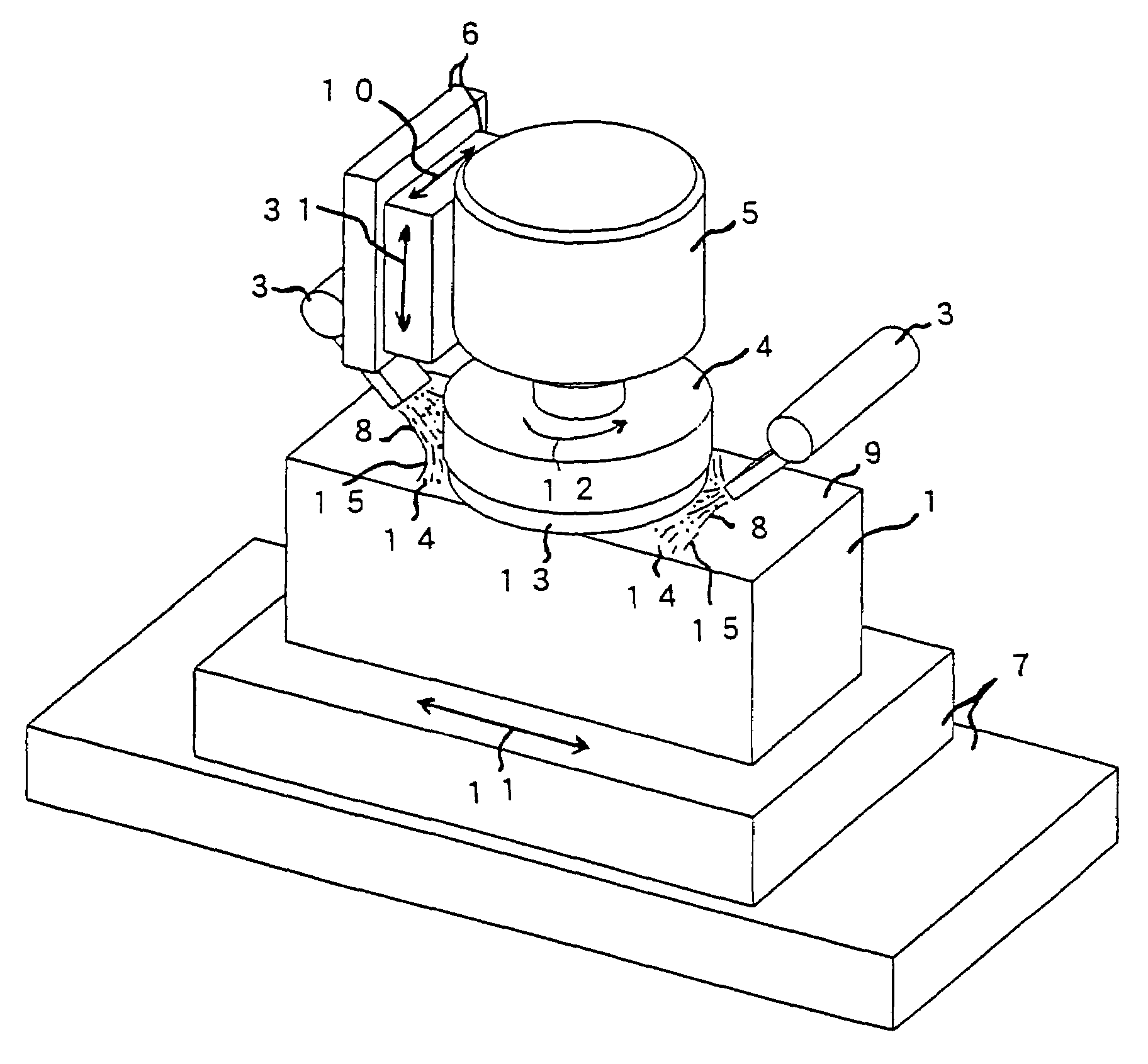
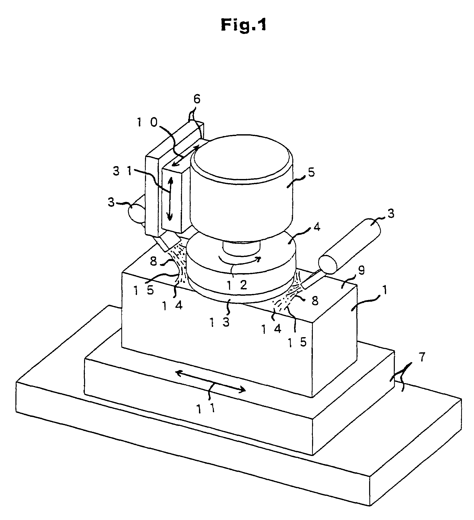
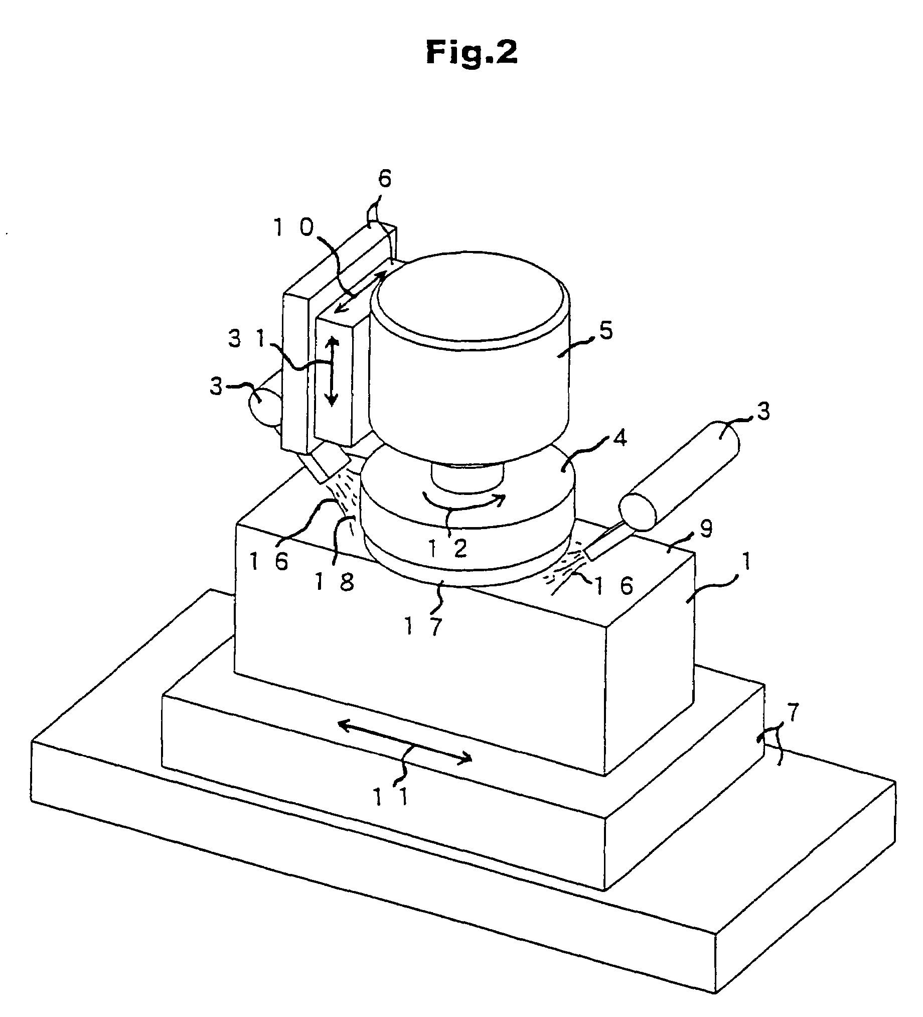
[0045]As shown in FIG. 4, a silicon block 1 was cut from a silicon ingot using a band saw 20. FIG. 4 shows a side face 19 of the silicon block and an edge 21 of the silicon block.

[0046]Four side faces 19 of the silicon block 1 were flattened by the method of the present invention to reduce defective wafers cracked in a later step and thus improve yield of the silicon wafer.

example 2

Method 1

[0047]The silicon block 1 of 125×125×250 mm obtained in Example 1 was polished by Method 1 to confirm the effect of the invention. A sponge wheel and a mixture of GC abrasive grains (#800) with polish oil were used as the polishing member 13 and the slurry 8, respectively.

[0048]As a result, four side faces 9 were polished in 16 minutes. Surface roughness Ry of the side faces was reduced from 20 μm to 5.8 μm by the polishing.

example 3

Method 1, Using Resin Brush

[0049]The silicon block 1 of 125×125×250 mm obtained in Example 1 was polished by Method 1 to confirm the effect of the invention. As the polishing member 13, a wheel (240 mm in diameter) provided with nylon resin hairs (0.5 mm in diameter, 20 mm in length) densely fixed with an epoxy adhesive on a bottom region of 160-240 mm diameter was used. As the slurry 8, a mixture of GC abrasive grains (#800) and polish oil (weight ratio 1:1.28) was used.

[0050]The polishing member 13 was pressed on the surface of the silicon block 1 to such a degree that the distal ends of the nylon resin hairs reach 1.5 mm below a position where the distal ends contact the surface of the silicon block 1. Then, the polishing member was rotated at 1800 rpm.

[0051]After the polishing member 13 contacted the surface of the silicon block 1, the silicon block 1 was moved along a lengthwise direction of the silicon block, which is orthogonal to a rotation axis of the polishing member 13. T...


PUM

PropertyMeasurementUnit
surface roughness Ryaaaaaaaaaa
lengthaaaaaaaaaa
sizeaaaaaaaaaa

Abstract

A method of manufacturing a solar cell including a silicon wafer is provided. In certain example instances, the method may include flattening fine roughness existing on a side face of a silicon block or a silicon stack used for manufacturing the silicon wafer for use in the solar cell.

Description

CROSS-REFERENCE TO RELATED APPLICATION[0001]This application is a continuation-in-part (CIP) of U.S. Ser. No. 10 / 716,661, filed Nov. 20, 2003, now abandoned, which is a division of 09 / 956,113, filed Sep. 20, 2001, now U.S. Pat. No. 6,679,759,the entire contents of which are hereby incorporated herein by reference. This application is also related to Japanese application Nos. 2000-296628 and 2001-272356, filed on Sep. 28, 2000 and Sep. 7, 2001, whose priority is claimed under 35 USC § 119, the disclosures of which are hereby incorporated herein by reference.BACKGROUND OF THE INVENTION[0002]1. Field of the Invention[0003]The present invention relates to a method of manufacturing a solar cell comprising a silicon wafer. In particular, it relates to a polishing technique for flattening fine roughness existing on a side face of a silicon block or a silicon stack.[0004]2. Description of Related Art[0005]Demand for silicon wafers is increasing year by year in accordance with the spread of ...

Claims


Application Information

Patent Timeline
Patent Type & Authority Patents(United States)
IPC IPC(8): B24B1/00
CPCB28D5/04B24B37/042
Inventor KAJIMOTO, KIMIHIKOWAKUDA, JUNZOU
Owner SHARP KK
Why Eureka
Try Eureka