Keyboard device

a keyboard and diode technology, applied in the field of keyboard devices, can solve the problems of increasing the cost of the keyboard device, the ineffective cost of the diode, and the inability to install the diode near the corresponding key intersection, so as to avoid the ghosting problem and low cost

Inactive Publication Date: 2020-01-09
PRIMAX ELECTRONICS LTD
View PDF3 Cites 1 Cited by
  • Summary
  • Abstract
  • Description
  • Claims
  • Application Information

AI Technical Summary

Benefits of technology

[0011]An object of the present invention provides a keyboard device with low cost and capable of avoiding the ghosting problem.
[0012]Another object of the present invention provides a keyboard device with reduced thickness and having a function of avoiding the ghosting problem.
[0016]From the above descriptions, the membrane switch circuit member of the keyboard device of the present invention is specially designed. The conductive paste marks are dispensed or sprayed on the first board, the second board or the circuit pattern to define the equivalent resistance. The equivalent resistance is effective to avoid the ghosting problem. Since the conductive paste marks are formed by the dispensing process or the spraying process, the layout area of the conductive paste marks can be easily increased or decreased. In other words, the equivalent resistances of the conductive paste marks can be adjusted according to the required resistance. In such way, the equivalent resistances of all conductive paste marks very close. Since the difference between the equivalent resistances of different conductive paste marks are not large, the problem of the conventional printing process is avoided. Moreover, since the keyboard device of the present invention is not equipped with the costly diodes, the fabricating cost of the keyboard device is reduced. Moreover, since the first contact and the second contact are separated from each other through the first insulation layer and the second insulation layer, it is not necessary to install the separation layer in the membrane switch circuit member. That is, the three-layered structure of the conventional membrane switch circuit member is replaced by the two-layered structure (i.e., the first board and the second board) of the membrane switch circuit member of the present invention. Consequently, the thickness of the keyboard device is reduced.

Problems solved by technology

However, the approach of installing diodes near the corresponding key intersection still has some drawbacks.
Firstly, the diode is not cost-effective.
Consequently, the cost of the keyboard device is increased.
The increased thickness of the membrane switch circuit member is detrimental to slimness of the keyboard device.
Thirdly, the process of welding the diodes at the positions near the corresponding key intersections is very complicated.

Method used


Image

  • Keyboard device
  • Keyboard device
  • Keyboard device

Examples


Embodiment Construction

[0024]For solving the drawbacks of the conventional technologies, the present invention provides a keyboard device.

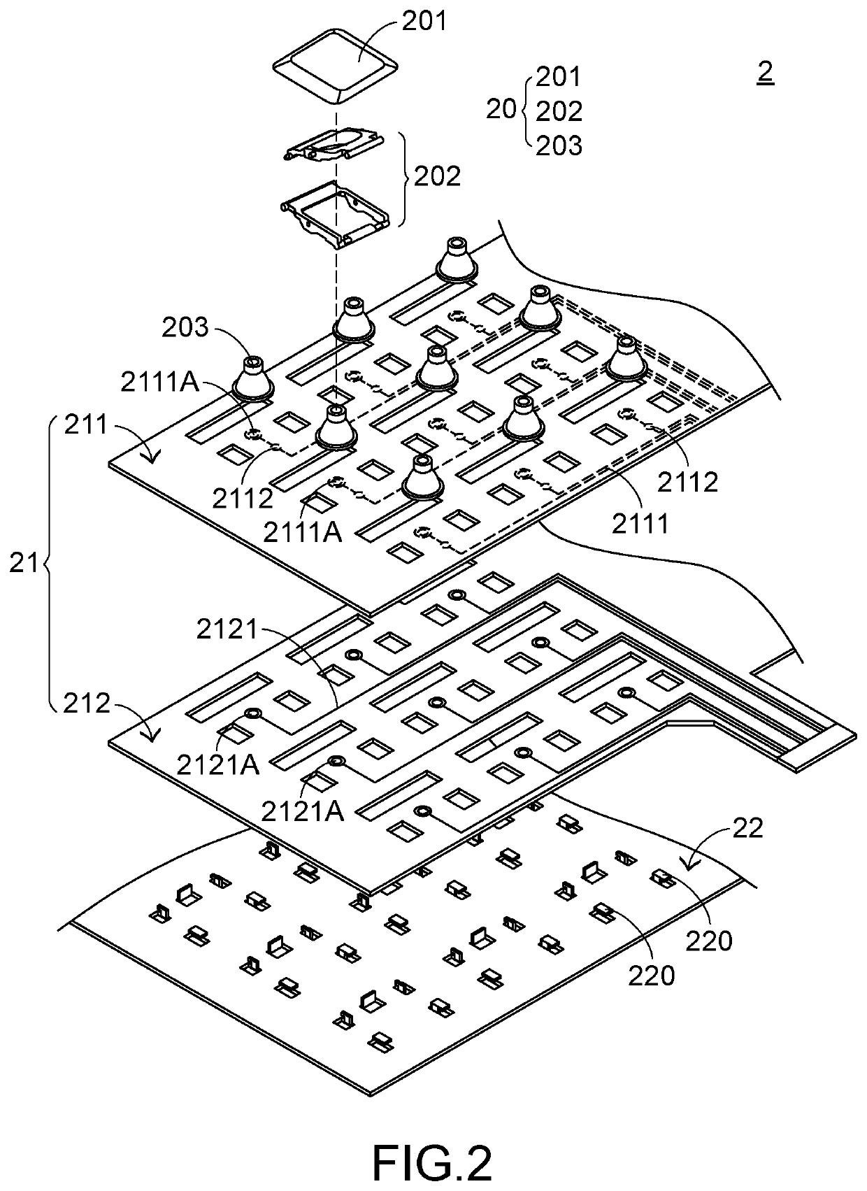
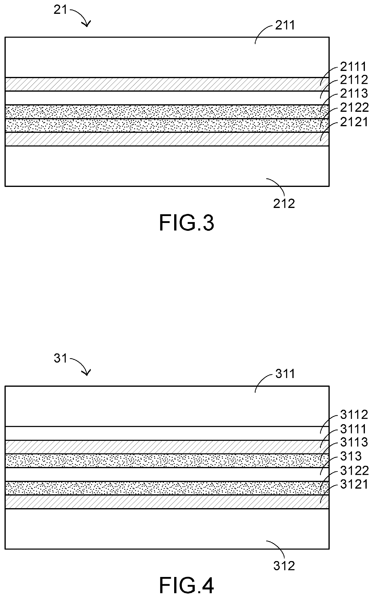
[0025]Hereinafter, the structure of the keyboard device of the present invention will be illustrated with reference to FIGS. 2 and 3. FIG. 2 is a schematic exploded view illustrating a portion of a keyboard device according to a first embodiment of the present invention. FIG. 3 is a schematic cross-sectional view illustrating a portion of a membrane switch circuit member of the keyboard device according to the first embodiment of the present invention. The keyboard device 2 comprises plural key structures 20, a membrane switch circuit member 21 and a base plate 22. The plural key structures 20 are exposed to a top surface of the keyboard device 2 and connected with the base plate 22. When one of the key structures 20 is depressed, the key structure 20 is moved downwardly relative to the base plate 22. Each key structure 20 comprises a keycap 201, a connecting element 20...


PUM


Abstract

A keyboard device includes a base plate, a key structure and a membrane switch circuit member. The membrane switch circuit member includes a first board and a second board. The first board includes a first circuit pattern, a conductive paste mark and a first insulation layer. The conductive paste mark is dispensed or sprayed on the first board or the first circuit pattern to define an equivalent resistance. Consequently, a ghosting problem is avoided. The second board includes a second circuit pattern and a second insulation layer. Since the first contact and the second contact are separated from each other through the first insulation layer and the second insulation layer, it is not necessary to install the separation layer in the membrane switch circuit member.

Description

CROSS-REFERENCE TO RELATED APPLICATION[0001]This application is a divisional application of application Ser. No. 15 / 878,973, filed Jan. 24, 2018, the content of which is incorporated by reference.FIELD OF THE INVENTION[0002]The present invention relates to a keyboard device, and more particularly to a keyboard device with a membrane switch circuit member.BACKGROUND OF THE INVENTION[0003]Generally, the widely-used peripheral input device of a computer system includes for example a mouse device, a keyboard device, a trackball device, or the like. Via the keyboard device, characters or symbols can be directly inputted into the computer system. As a consequence, most users and most manufacturers of input devices pay much attention to the development of keyboard devices.[0004]Hereinafter, a key structure with a scissors-type connecting element in a conventional keyboard will be illustrated with reference to FIG. 1. FIG. 1 is a schematic side cross-sectional view illustrating a convention...

Claims


Application Information

Patent Timeline
Patent Type & Authority Applications(United States)
IPC IPC(8): H01H13/705G06F3/02
CPCH01H13/705G06F3/0202H01H13/704H01H2203/028H01H2239/03
Inventor CHEN, BO-ANPAN, CHIN-SUNG
Owner PRIMAX ELECTRONICS LTD
Why Eureka
Try Eureka