
Anti-electromagnetic interference circuit board

Active Publication Date: 2020-01-09
ASUSTEK COMPUTER INC
View PDF6 Cites 0 Cited by
  • Summary
  • Abstract
  • Description
  • Claims
  • Application Information

AI Technical Summary

Benefits of technology

The patent is about a circuit board that helps reduce electromagnetic interference and improve signal transmission. The position of a magnetic conductor on the board can be adjusted to meet different users' needs. Different magnetic materials are used on the circuit board to further reduce electromagnetic waves. In simple terms, this patent helps make electronic devices safer and better.

Problems solved by technology

In addition, radiation between layers of the circuit board results in an electromagnetic compatibility (EMC) problem, which affects the transmitting quality of the high-speed signal in the circuit.
However, although the conventional method can solve the problems of capacitive and inductive effects, manufacturing costs of the circuit board are increased due to manufacturing of a blind hole and a buried hole.
A probability is also occurred that the board is bent and damaged caused by manufacturing a relatively thin board layer.

Method used


Image

  • Anti-electromagnetic interference circuit board

Examples


Embodiment Construction

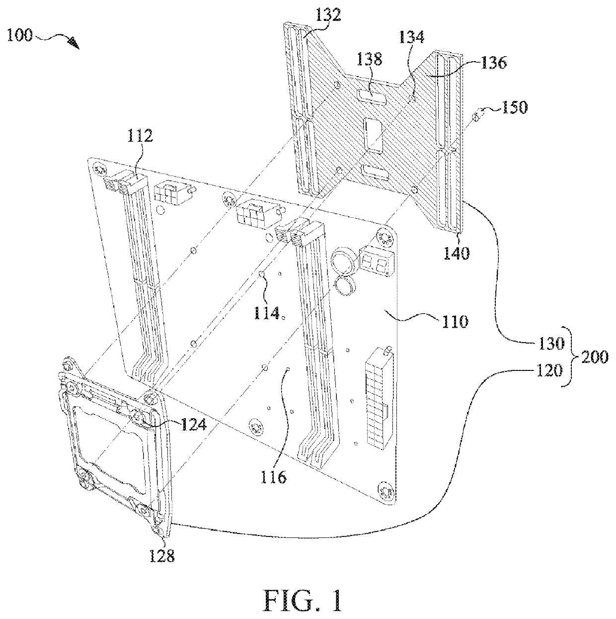
[0008]The following is a detailed description of the embodiments with reference to the accompanying drawings, which are not intended to limit the scope of this application, and the description of the operation of the structure is not intended to limit the order of execution thereof. Any device with the same effects shall fall within this application as long as its structure is merely recombination of components described herein. In addition, the drawings are for illustrative purposes only and are not drawn to the original dimensions. For ease of understanding, the same or similar elements in the following description are denoted by the same reference numerals.

[0009]Unless otherwise specified, all the terms as used herein generally have the same meaning as is commonly understood by persons skilled in the art. Some terms used for describing this application will be discussed below or in other parts of this specification, so as to provide additional guidance for persons skilled in the ...


PUM


Abstract

An anti-electromagnetic interference circuit board includes a circuit board and a magnetic conductor. The circuit board has a plurality of vias, and the magnetic conductor is covered on the circuit board to cover some of the vias. The magnetic conductor includes a plate, a carrier, a sprayed magnetic conductor, and a wave absorbing magnetic conductor.

Description

CROSS-REFERENCE TO RELATED APPLICATION[0001]This application claims the priority benefit of TW application serial No. 107209124, filed on Jul. 5, 2018. The entirety of the above-mentioned patent application is hereby incorporated by reference herein and made a part of the specification.BACKGROUND OF THE INVENTIONField of the Invention[0002]The disclosure relates a circuit board and more particularly, to an anti-electromagnetic interference circuit board.Description of the Related Art[0003]Because a circuit board layout is increasingly dense, in order to increase a wiring area, multi-layer boards are conducted. In the multi-layer boards, different circuit layers communicate with each other through vias. However, once a via is placed around the paths with a high-speed signal transmitting, capacitive and inductive effects are generated, and consequently a radiation magnetic field is generated from the via. In addition, radiation between layers of the circuit board results in an electro...

Claims


Application Information

Patent Timeline
IPC IPC(8): H05K1/02H05K9/00
CPCH05K9/002H05K1/115H05K2201/10371H05K1/0233H05K9/0033H05K1/0222
Inventor TSOU, PING-HANWAN, LI-CHIEN
Owner ASUSTEK COMPUTER INC
Learn More