Circuit board module and method of assembling circuit board module

a circuit board module and circuit board technology, applied in the field of circuit board modules, can solve the problems that the wires connecting the connector with the communication ics cannot always be shortest, and the difference in communication quality can accordingly be increased, so as to reduce the number of wires connected to the connector, increase the freedom of circuit pattern design, and reduce the effect of wiring

Inactive Publication Date: 2020-02-27
DENSO CORP
View PDF11 Cites 1 Cited by
  • Summary
  • Abstract
  • Description
  • Claims
  • Application Information

AI Technical Summary

Benefits of technology

[0010]In general, when a connector is shared by communication ICs mounted on both sides of the circuit board to be used in different communication circuits, respectively, because an impedance of wiring that connects the connector with a communication IC mounted on an opposite side to the connector varies, a communication quality via the wiring decreases. In particular, when the communication ICs are mounted on the same side of the circuit board, an area to be able to form the circuit patterns from the terminals of the connector to the respective communication ICs can be limited depending on either a size of an area of the circuit board occupied by the communication ICs or specifications (e.g., a size, a layout of terminals, etc.) of the communication ICs as well. Hence, due to a difference in impedance between the circuit patterns, a difference in communication quality can accordingly be increased as a problem. However, according to the above-described system (i.e., the configuration), the first communication IC is mounted on the first side of the sensor circuit board, and the second communication IC is mounted on the second side of the sensor circuit board. That is, since respective circuit patterns extending from the connector to the first and second communication ICs can be formed on different sides of the sensor circuit board, freedom of designing the circuit patterns can be increased regardless of the size of the area of the circuit board occupied by the first and second communication ICs and any devices needed for communication wiring thereon. As a result, since the difference in communication quality between communications executed by the respective communication ICs can be minimized, a single connector can be preferably used.

Problems solved by technology

However, when the communication ICs are mounted on the same side of the circuit board, all of the wires connecting the connector with the communication ICs cannot always be shortest.
Hence, due to a difference in impedance between the circuit patterns, a difference in communication quality can accordingly be increased as a problem.

Method used


Image

  • Circuit board module and method of assembling circuit board module
  • Circuit board module and method of assembling circuit board module
  • Circuit board module and method of assembling circuit board module

Examples


Embodiment Construction

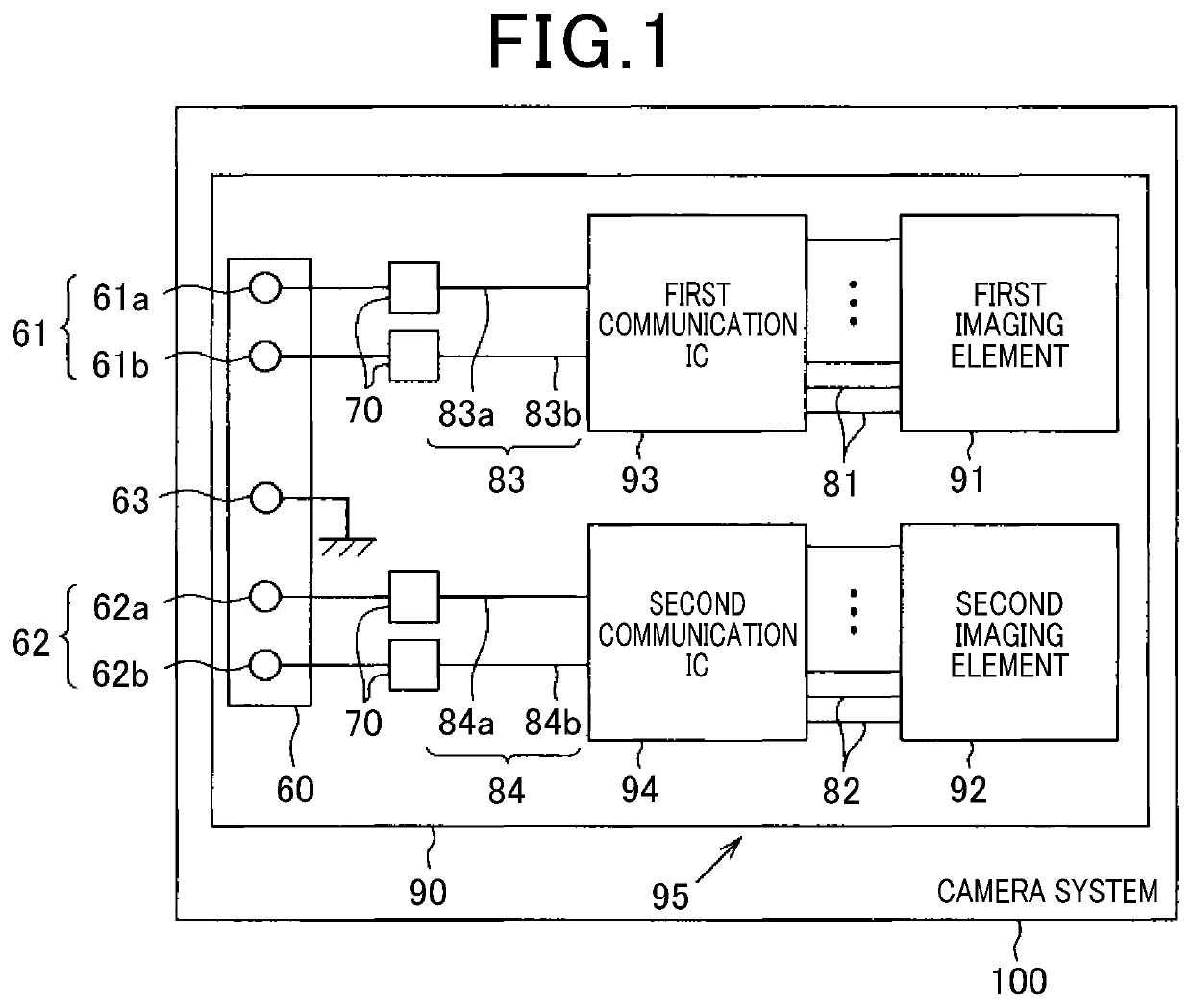
[0017]Referring now to the drawings, wherein like reference numerals designate identical or corresponding parts throughout the several views thereof, and to FIG. 1, an exemplary camera system mounted on a vehicle according to a first embodiment of the present disclosure is described. That is, a camera system is installed, for example, in a vehicle to capture an image of surroundings of an own vehicle and outputs image data to a camera ECU (Electric Control Unit).

[0018]The camera system 100 of FIG. 1 includes a lens section (not illustrated) that acts as an optical system and a circuit board module 95 that converts light focused by the lens section into an image signal. The circuit board module 95 includes a sensor circuit board 90 of a both-side mounted type, on each of which one or more elements are mountable. For example, a first imaging element 91, a second imaging element 92, and a first communication IC 93 are mounted on the sensor circuit board 90. Also, a second communication...


PUM


Abstract

To provide a circuit board module capable of effectively performing input and output to and from more than two communication ICs by using only one female connector having multiple terminals, the multiple terminals include at least one first terminal 61 connected to a first circuit pattern 83a on a first side 90a of the sensor circuit board 90 and at least one second terminal 62 connected to a second circuit pattern 84a on a second side 90b thereof. The at least one first terminal 61 includes an overlapping portion 50 at its tip to be laid on the first side 90a and is connected to the first circuit pattern 90a thereon. The at least one second terminal 62 includes a penetrating portion 52 at its tip to penetrate the sensor circuit board 90 and is connected to the second circuit pattern 84a on the second side 90b.

Description

CROSS-REFERENCE TO RELATED APPLICATION[0001]This patent application is based on and claims priority to Japanese Patent Application 2018-156146, filed on Aug. 23, 2018 in the Japan Patent Office, the entire disclosure of which is hereby incorporated by reference herein.BACKGROUNDTechnical Field[0002]Embodiments of this disclosure relate to a circuit board module having a connector mounted on any one of sides of the circuit board, and a method of assembling the circuit board module.Related Art[0003]A conventional circuit board module is composed of a circuit board and a connector with multiple terminals mounted on the circuit board. Each of the terminals of the connector is physically connected to a circuit pattern formed on the circuit board and is electronically connected to the circuit board via the circuit pattern.[0004]When multiple communication ICs (Integrated Circuits) are mounted on a circuit board and a single connector is shared, wires that connect the communication ICs wit...

Claims


Application Information

Patent Timeline
Patent Type & Authority Applications(United States)
IPC IPC(8): H05K5/00H05K7/10H05K1/11
CPCH05K5/0069H05K7/10H05K1/115H05K1/18H05K1/184H05K5/0065H05K2201/10189
Inventor KIMATA, TETSUYA
Owner DENSO CORP
Why Eureka
Try Eureka