MEMS device having a rugged package and fabrication process thereof

a technology of micro-electromechanical system and rugged packaging, which is applied in the direction of piezoelectric/electrostrictive devices, decorative arts, chemical vapor deposition coatings, etc., can solve the problems of not being able to protect the movement sensor, not being able to increase the robustness of the mems device, and undesired impact, etc., to achieve the effect of loss of generality

Inactive Publication Date: 2020-04-16
STMICROELECTRONICS SRL
View PDF0 Cites 1 Cited by
  • Summary
  • Abstract
  • Description
  • Claims
  • Application Information

AI Technical Summary

Benefits of technology

[0014]Embodiments are directed to a MEMS device and a fabrication process thereof. In particular, the present disclosure relates to a MEMS (Micro Electro-Mechanical System) device having a rugged package and to the fabrication process thereof. More particularly, reference is made hereinafter to a packaging process that uses an injection molding system. Moreover, hereinafter reference is made to MEMS devices comprising one or more MEMS sensors capable of detecting movements (such as accelerometers), without this implying any loss of generality.

Problems solved by technology

In most cases, it is not desirable to increase the robustness of MEMS devices by increasing their dimensions.
Since the resonance frequency is an important parameter for determining the performance of the MEMS device, it is not desirable to improve the robustness of the MEMS device by modifying its dimensions since this would have an undesired impact on performance.
However, known solutions have some disadvantages.
In fact, if subjected to repeated mechanical shocks with high accelerations, mechanical stoppers of a MEMS movement sensor undergo gradual damage and failure, causing failure of the mechanical stoppers in the long run, which thus no longer protect the MEMS movement sensor.
These repeated accelerations may lead to malfunctioning or failure of the MEMS device, thus rendering it unusable.
This problem is particularly felt when handling the MEMS device before assembling the package (in particular, fixing the MEMS device to a supporting structure).

Method used


Image

  • MEMS device having a rugged package and fabrication process thereof
  • MEMS device having a rugged package and fabrication process thereof
  • MEMS device having a rugged package and fabrication process thereof

Examples


Embodiment Construction

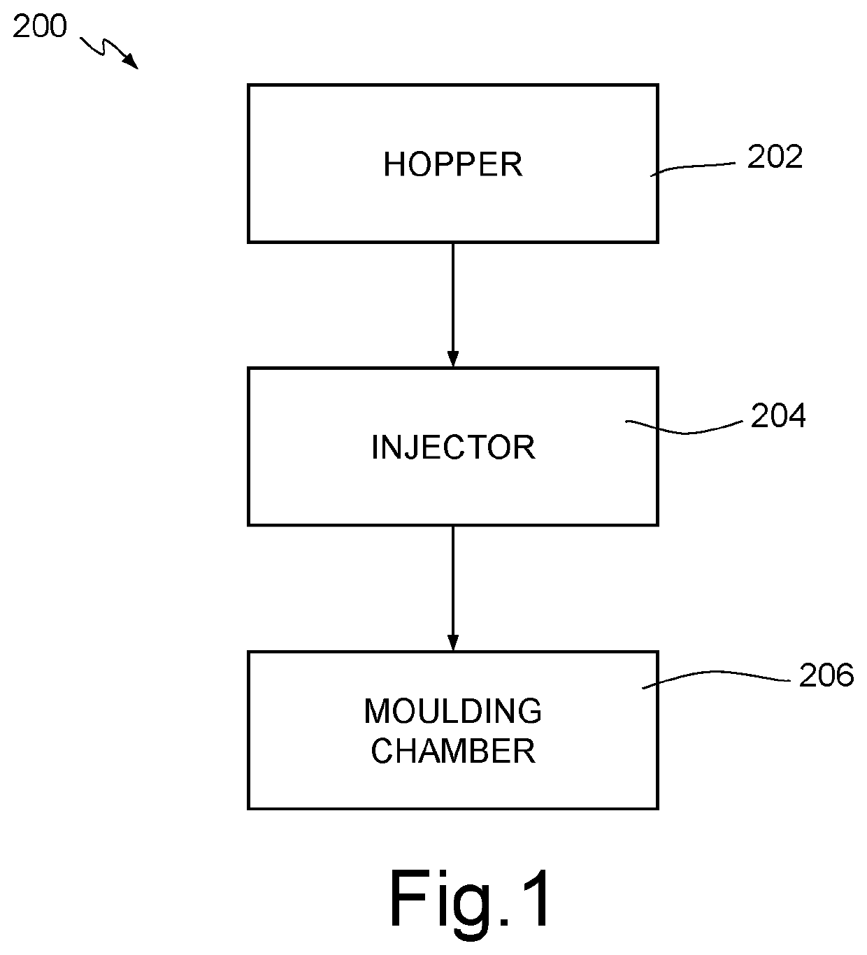
[0021]FIG. 1 schematically illustrates an injection molding system, hereinafter referred to as system 200.

[0022]In particular, the system 200 comprises a hopper 202, which supplies a material to be injected in solid form (for example, in the form of pellets); an injector 204, provided with a heater and an injection system (not illustrated); and a molding chamber 206, housing one or more wafers or devices to be processed and comprising one or more molding matrices (not illustrated).

[0023]In use, in the molding chamber 206, the aforementioned one or more molding matrices are fixed to the wafer or to the device to be processed. In particular, the molding matrix or matrices have one or more cavities, which define the desired shape for the element to be molded on the wafer or on the device to be processed.

[0024]The hopper 202 supplies the material to be injected to the injector 204, which, through the heater, heats it up to the melting point (or, in case of plastic materials, the point o...


PUM

PropertyMeasurementUnit
Young's modulusaaaaaaaaaa

Abstract

A MEMS device formed by a substrate, having a surface; a MEMS structure arranged on the surface; a first coating region having a first Young's modulus, surrounding the MEMS structure at the top and at the sides and in contact with the surface of the substrate; and a second coating region having a second Young's modulus, surrounding the first coating region at the top and at the sides and in contact with the surface of the substrate. The first Young's modulus is higher than the second Young's modulus.

Description

BACKGROUNDTechnical Field[0001]The present disclosure relates to a MEMS (Micro Electro-Mechanical System) device and the fabrication process thereof.Description of the Related Art[0002]As is known, electronic apparatuses comprising MEMS devices, such as MEMS movement sensors, are increasingly widespread. For the correct operation of such apparatuses, it is desired that MEMS devices are capable of detecting movement variations in an accurate and precise way in all operating conditions. Consequently, it is desirable for MEMS devices to be sufficiently sturdy so as not to break even when they are subjected to abrupt movements (for example, as a result of the apparatus being dropped or undergoing mechanical shock). Furthermore, it is desirable that their performance not to be significantly affected by the above abrupt movements.[0003]In most cases, it is not desirable to increase the robustness of MEMS devices by increasing their dimensions. In fact, MEMS movement sensors may be modelle...

Claims


Application Information

Patent Timeline
Patent Type & Authority Applications(United States)
IPC IPC(8): B81C1/00B81B3/00B81C99/00
CPCB81C1/00325B81C99/0005B81B3/0018B81C2201/112B81B7/0048B81B7/0058B81B2201/0235B81B2207/012B81C2203/0136B81C2203/0154
Inventor DUQI, ENRIDEL SARTO, MARCOBALDO, LORENZO
Owner STMICROELECTRONICS SRL
Why Eureka
Try Eureka