Interconnect structure having reduced resistance variation and method of forming same

a technology of resistance variation and interconnect structure, which is applied in the direction of basic electric elements, semiconductor/solid-state device manufacturing, electric devices, etc., can solve the problems of losing performance improvement, and achieve the effect of reducing resistance variation

Active Publication Date: 2020-05-07
GLOBALFOUNDRIES US INC
View PDF2 Cites 2 Cited by
  • Summary
  • Abstract
  • Description
  • Claims
  • Application Information

AI Technical Summary

Benefits of technology

This patent discusses a method to create interconnect structures with reduced resistance variation. The method involves using a hardmask layer between metal lines in a dielectric layer to improve the accuracy of the metal lines. This results in a more reliable and efficient interconnect structure. The technical effects of this patent are improved performance and reliability of the interconnect structure, which is important for the development of advanced electronic devices.

Problems solved by technology

While transistor speeds continue to improve with scaling, the challenge for interconnect scaling is to not become a bottleneck and lose that performance improvement.

Method used


Image

  • Interconnect structure having reduced resistance variation and method of forming same
  • Interconnect structure having reduced resistance variation and method of forming same
  • Interconnect structure having reduced resistance variation and method of forming same

Examples


Embodiment Construction

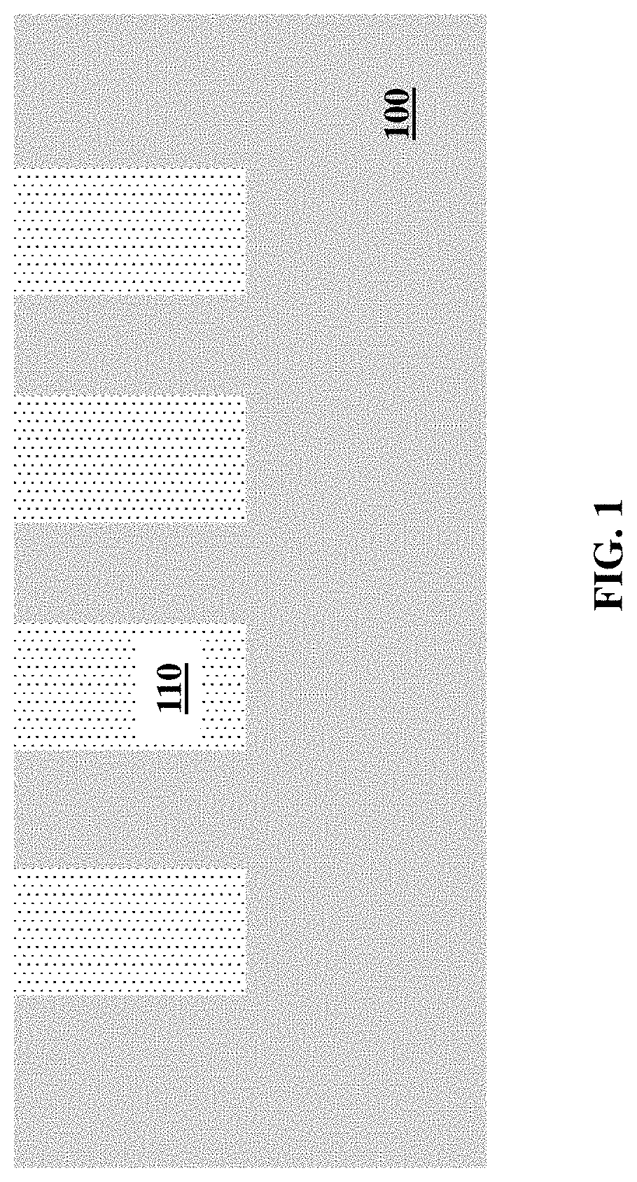
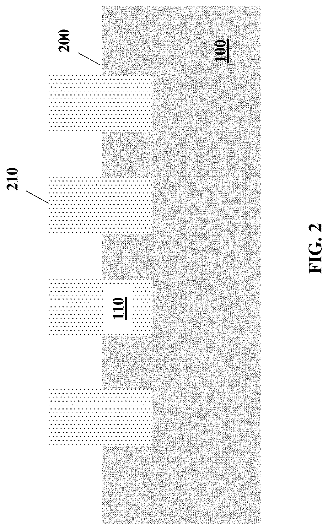
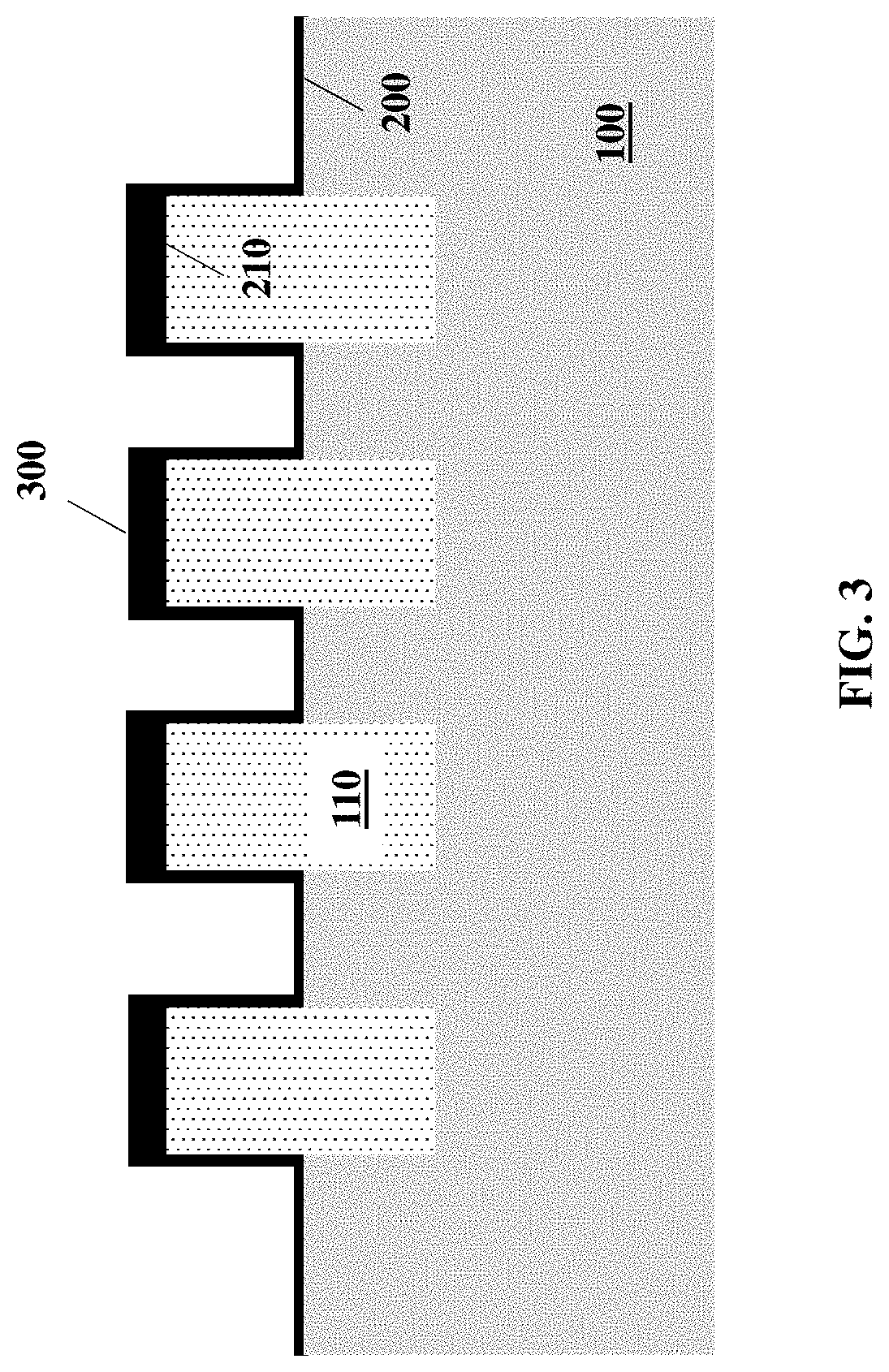
[0019]The subject matter disclosed herein relates to an interconnect structure of an integrated circuit (IC) having reduced resistance variation. More specifically, various aspects described herein relate to an interconnect structure of an IC that includes a hardmask layer between metal lines and has reduced resistance variation, and a method of forming the same.

[0020]As noted above, as conventional ICs continue to scale down (such as to the 7 nm technology node and beyond), interconnect scaling continues downward as well. However, as also noted above, one challenge for such interconnect scaling is to keep RC low so as to not hinder transistor speed improvement that comes along with scaling down. Various aspects of the disclosure include methods of forming interconnect structures which prevent degradation of resistance performance and thereby reduce variability of interconnect resistance, thus keeping interconnect RC low. In other aspects of the disclosure, interconnect structures a...


PUM

PropertyMeasurementUnit
sizesaaaaaaaaaa
dielectricaaaaaaaaaa
resistanceaaaaaaaaaa

Abstract

An interconnect structure of an integrated circuit and a method of forming the same, the interconnect structure including: at least two metal lines laterally spaced from one another in a dielectric layer, the metal lines having a top surface below a top surface of the dielectric layer; a hardmask layer on an upper portion of sidewalls of the metal lines, the hardmask layer having a portion extending between the metal lines, the extending portion being below the top surface of the metal lines; and at least one fully aligned via on the top surface of a given metal line.

Description

TECHNICAL FIELD[0001]The subject matter disclosed herein relates to an interconnect structure of an integrated circuit (IC) having reduced resistance variation. More specifically, various aspects described herein relate to an interconnect structure of an IC that includes a hardmask layer between metal lines and has reduced resistance variation, and method of forming the same.BACKGROUND[0002]As integrated circuits (ICs) continue to scale downward in size, transistors and interconnects have also had to become smaller and smaller. However, in scaled down sizes such as at the 7 nanometer (nm) technology node and beyond, scaling faces the so-called “RC challenge” (R=electrical resistance, C=capacitance). While transistor speeds continue to improve with scaling, the challenge for interconnect scaling is to not become a bottleneck and lose that performance improvement. Thus, the product of resistance and capacitance (RC) needs to remain low during interconnect scaling in order to create fa...

Claims


Application Information

Patent Timeline
Patent Type & Authority Applications(United States)
IPC IPC(8): H01L21/768
CPCH01L21/76804H01L21/76831H01L21/76897H01L21/76885H01L21/76834H01L21/76837
Inventor LICAUSI, NICHOLAS V.PARK, CHANROXIE, RUILONGLABONTE, ANDRE P.
Owner GLOBALFOUNDRIES US INC
Why Eureka
Try Eureka