Resistive radom access memory device, method for manufacturing the same, and method for operating the same

a resistive random access and memory device technology, applied in the field of memory devices, can solve the problems of limited memory performance, limiting memory performance, and limiting the operation of resistive random access memory devices in 1d-1r configuration, and achieves the effects of improving memory performance, small wafer footprint, and high switching speed

Active Publication Date: 2013-05-23
PEKING UNIV
View PDF5 Cites 22 Cited by
  • Summary
  • Abstract
  • Description
  • Claims
  • Application Information

AI Technical Summary

Benefits of technology

[0021]The resistive random access memory device according to the present disclosure has 1D-1R configuration and operates in bipolar resistive switching scheme. It occupies a relatively small footprint of a wafer, such as 4F2, where F represents a feature size. Moreover, it has improved memory performances when compared with unipolar resistive random access memory devices, such as high switching speed, small erasing current, small resistance, small voltage variations, long data retention time and high reliability.
[0022]The Schottky diode in the resistive random access memory device is faster than other types of diodes, which can further increase operation speed and reliability. Moreover, the Schottky diode has current density larger than other types of diodes and can limit a current during programming operation, which can further increase endurance and reduce resistance variation.
[0023]The Schottky diode has desired value of reverse saturation current by precisely tuning doping of the semiconductor layer. Furthermore, a process for forming a Pt—Si based Schottky diode is simple and compatible to conventional semiconductor processes. Thus, the resistive random access memory device according to the present disclosure can be mass-produced.
[0024]By limiting voltages for read operation, programming operation and erasing operation in specific ranges, an unintended read operation on an adjacent resistive random access memory can be avoided when operating a selected resistive random access memory. A plurality of resistive random access memory devices according to the present disclosure can be arranged an array with a high density. Each of the plurality of resistive random access memory devices is located at a cross point of a bit line and a word line as a memory cell.

Problems solved by technology

Because the select transistor is used, it occupies a major portion of a footprint of the memory cell, which hinders an increase of the integration level.
However, conventional resistive switching memory devices in 1D-1R configuration can only operate in unipolar resistive switching scheme due to limited material properties of the diode, which in turn limits memory performances.

Method used


Image

  • Resistive radom access memory device, method for manufacturing the same, and method for operating the same
  • Resistive radom access memory device, method for manufacturing the same, and method for operating the same
  • Resistive radom access memory device, method for manufacturing the same, and method for operating the same

Examples


Embodiment Construction

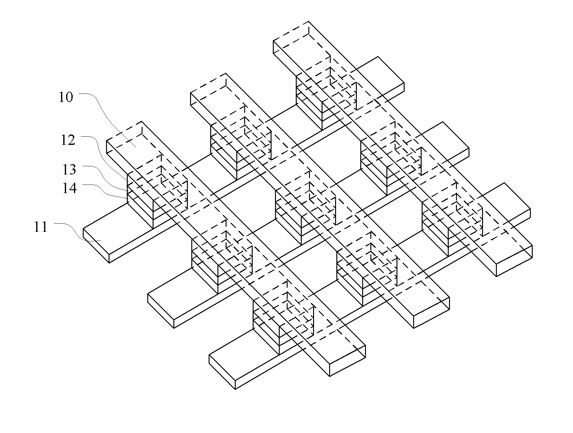
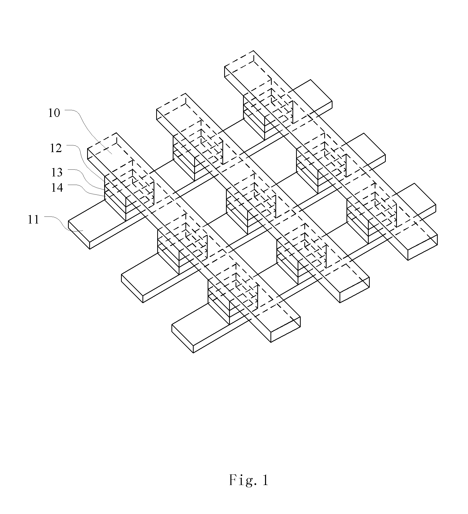
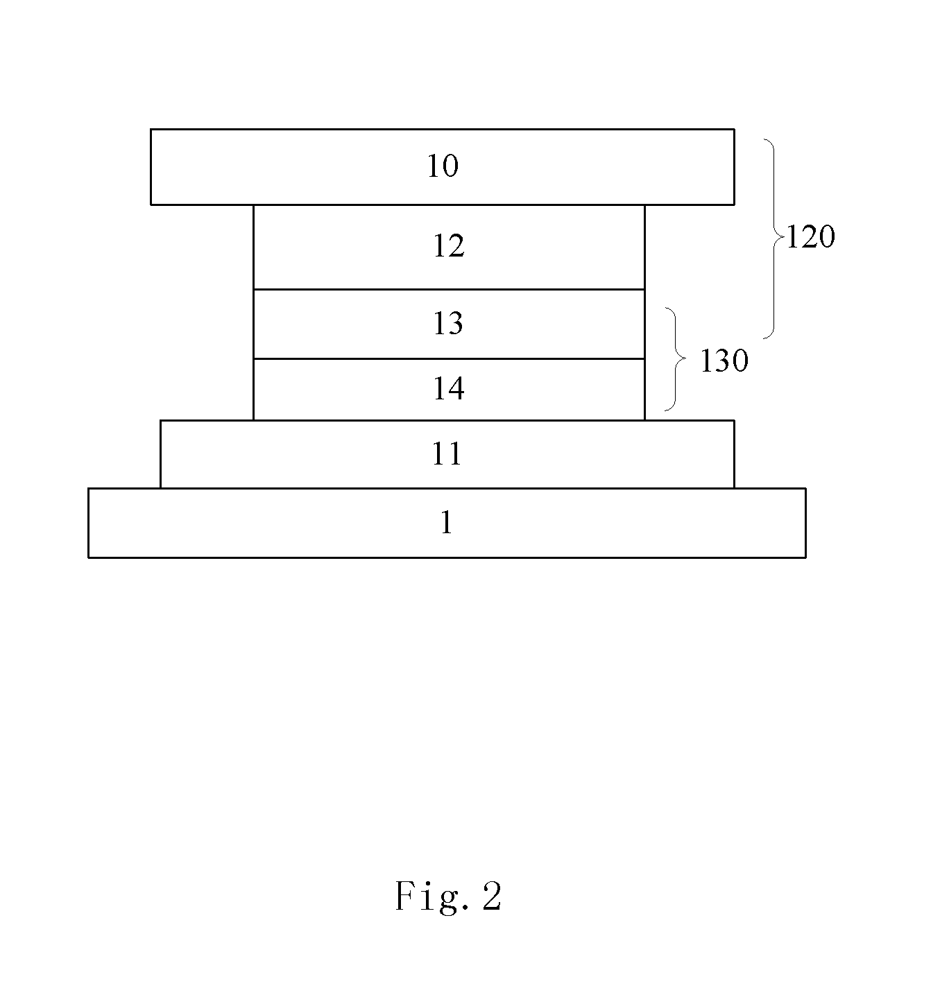
[0030]Exemplary embodiments of the present disclosure will be described in more details below with reference to the accompanying drawings. In the drawings, like reference numerals denote like members. The figures are not drawn to scale, for the sake of clarity.

[0031]It should be understood that when one layer or region is referred to as being “above” or “on” another layer or region in the description of device structure, it can be directly above or on the other layer or region, or other layers or regions may be intervened therebetween. Moreover, if the device in the figures is turned over, the layer or region will be “under” or “below” the other layer or region.

[0032]In contrast, when one layer is referred to as being “directly on” or “on and adjacent to” or “adjoin” another layer or region, there are not intervening layers or regions present.

[0033]In the present application, the term “semiconductor structure” means generally the whole semiconductor structure formed at each step of ...


PUM

PropertyMeasurementUnit
thicknessaaaaaaaaaa
thicknessaaaaaaaaaa
reverse saturation currentaaaaaaaaaa

Abstract

A resistive random access memory device, a method for manufacturing the resistive random access memory device, and a method for operating the resistive random access memory device are disclosed. The resistive random access memory device includes a resistive switching memory element including two electrodes and a layer of variable-resistance material between the two electrodes, wherein the layer of variable-resistance material exhibits bipolar resistive switching behavior; and a Schottky diode including a metal layer and a p-doped semiconductor layer which contact each other, wherein the metal layer of the Schottky diode is coupled to one of the two electrodes of the resistive switching memory element. The present disclosure provides the resistive random access memory device operating in bipolar resistive switching scheme.

Description

TECHNICAL FIELD[0001]The present disclosure relates to a memory device, and in particular, to a resistive random access memory device (RRAM).[0002]The present disclosure also relates to a method for manufacturing the resistive random access memory device and a method for operating the resistive random access memory device.BACKGROUND[0003]Today, advance of microelectronic industry also promotes memory technology to achieve an increased integration level and a reduced manufacture cost. Non-volatile memory devices maintain information data stored therein after power off and play an important role in information storage.[0004]One of novel non-volatile memory devices uses a variable-resistance material and has the advantages of high operation speed (<5 ns), low power dissipation (<1V) and easily being integrated with other semiconductor devices. Such non-volatile memory devices are a prospective candidate for next-generation memory devices. The resistive switching memory device typ...

Claims


Application Information

Patent Timeline
Patent Type & Authority Applications(United States)
IPC IPC(8): G11C13/00H01L45/00
CPCG11C13/0007G11C13/003G11C13/0069G11C2013/0073G11C2213/72G11C2213/76H01L45/1608H01L27/2463G11C13/0002H01L45/1253H01L45/16G11C2213/15H01L27/2409H10B63/20H10B63/80H10N70/021H10N70/011H10N70/841
Inventor KANG, JINFENGGAO, BINCHEN, YUANSHASUN, BINGLIU, LIFENGLIU, XIAOYAN
Owner PEKING UNIV
Why Eureka
Try Eureka