Nonvolatile memory erase method and device

A non-volatile memory, over-erasing technology, applied in the erasing device of non-volatile memory devices, the erasing field of non-volatile memory, can solve the problems of long Pre_PGM time, affecting the erasing speed, etc., to reduce risks , saving time, improving erase speed and memory performance

Active Publication Date: 2013-12-04
GIGADEVICE SEMICON (BEIJING) INC
View PDF2 Cites 17 Cited by
  • Summary
  • Abstract
  • Description
  • Claims
  • Application Information

AI Technical Summary

Problems solved by technology

[0008] First, because the reference PV state corresponds to a higher threshold, which means that the Pre_PGM time is longer, especially for those few cells located near the PV state, so this will affect the entire erasing speed;
[0009] Second, for those cells with a higher threshold, it may cause Over Program (over-programming), and when these over-programmed cells are erased, it will take more wasted time, which also affects the erase In addition to speed

Method used


Image

  • Nonvolatile memory erase method and device
  • Nonvolatile memory erase method and device
  • Nonvolatile memory erase method and device

Examples


Embodiment Construction

[0040] In order to make the above objects, features and advantages of the present application more obvious and comprehensible, the present application will be further described in detail below in conjunction with the accompanying drawings and specific implementation methods.

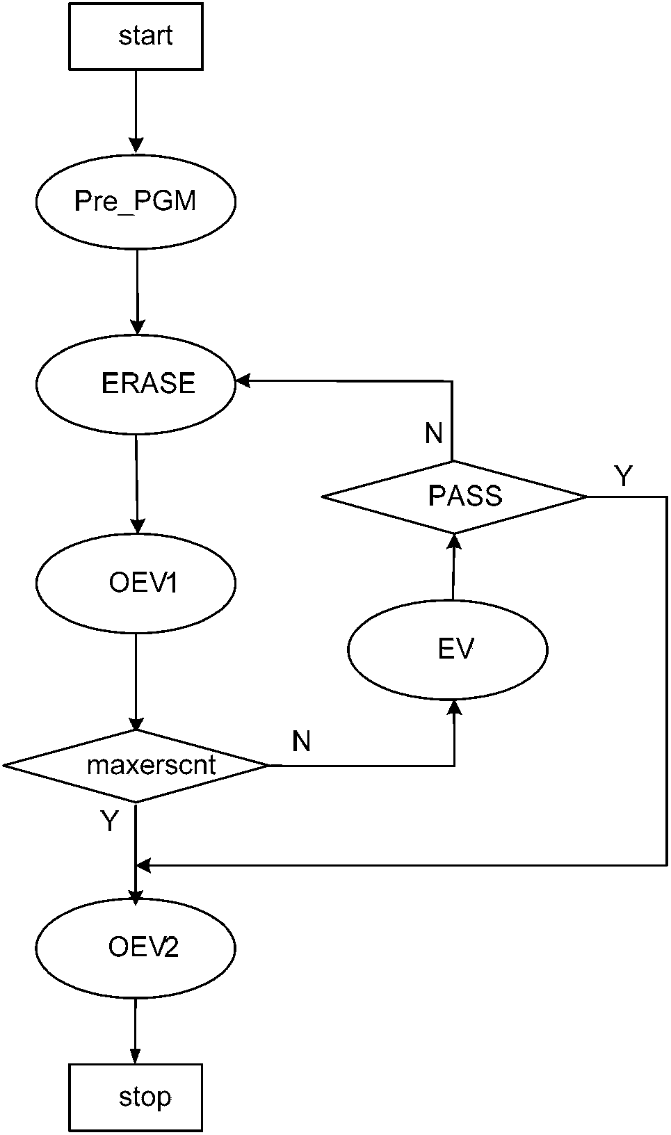
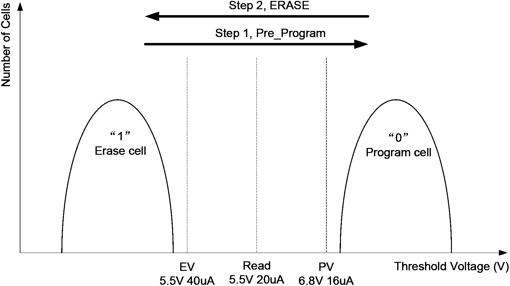
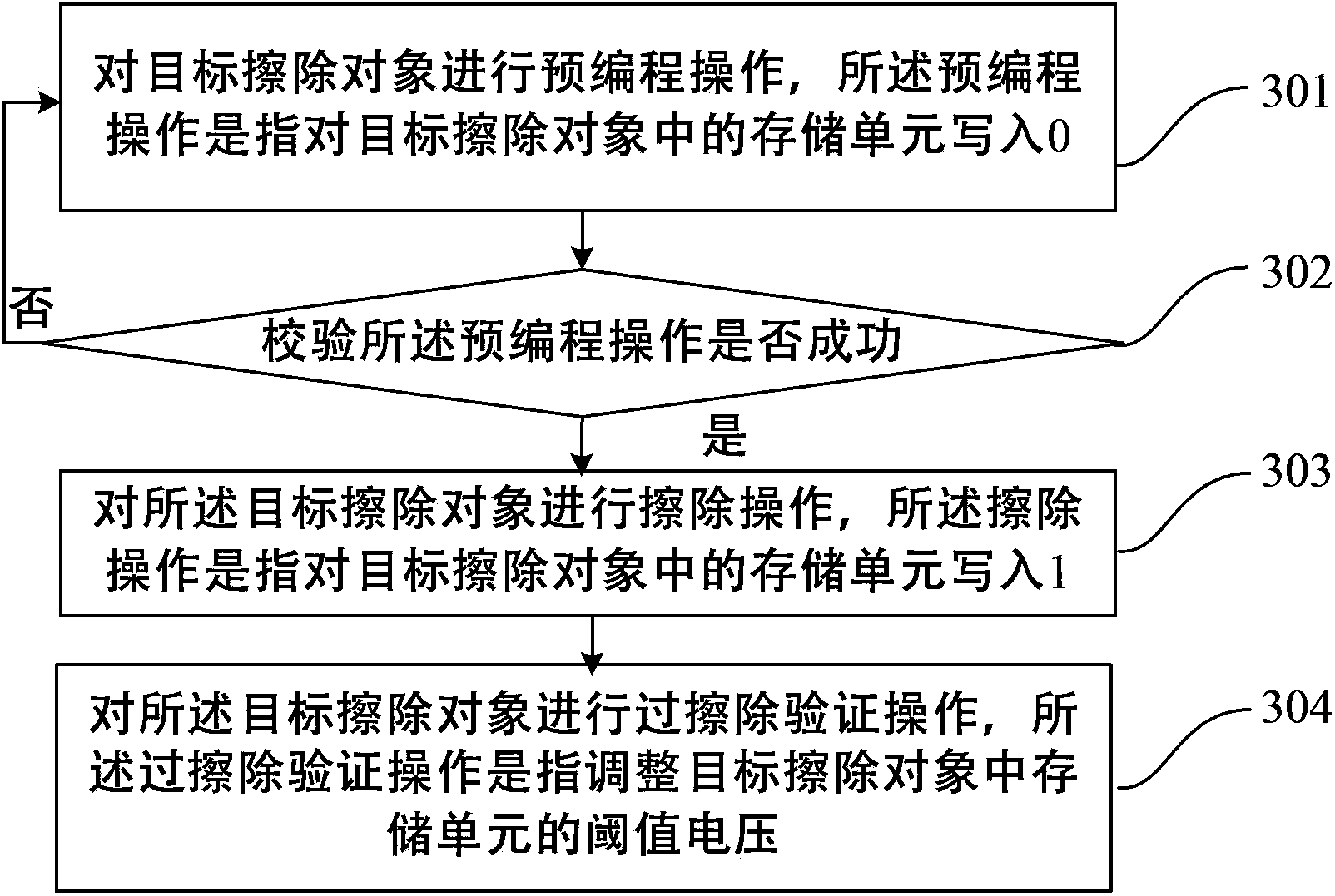
[0041] With the rapid development and wide application of various electronic devices and embedded systems, such as computers, personal digital assistants, mobile phones, digital cameras, etc., there is a great need for a device that can be programmed many times, has a large capacity, is fast to read and write, and can be erased. Convenient, simple, less peripheral devices, low-cost non-volatile (can still maintain the stored data information in the case of power failure) storage device. The non-volatile memory device emerges as the times require under this background demand. The core of a non-volatile memory is an array of memory cells. A memory cell is usually a floating gate device that can store charg...


PUM


Abstract

The invention discloses a nonvolatile memory erase method and a nonvolatile memory erase device. The method comprises the steps that: a target erasing target is subjected to a preprogramming operation, wherein the preprogramming operation is that 0 is written into memory units of the target erase object; whether the preprogramming operation is successful is examined, wherein the examining is that whether currents of the memories in the target erase object processed through the preprogramming operation under a certain gate voltage are all smaller than a target current value which is a current value with current margin; if the preprogramming operation is successful, a next step is executed, and if not, the progress is turned back to the execution of the preprogramming operation; the target erase object is subjected to an erase operation, wherein the erase operation is that 1 is written into memory units of the target erase object; and the target erase object is subjected to an over-erase examine operation, wherein the over-erase examine operation is that threshold voltage of memory units in the target erase object is adjusted. With the method and device provided by the invention, nonvolatile memory erase speed can be improved, and memory performance can be improved.

Description

technical field [0001] The present application relates to the technical field of semiconductor memory, in particular to a method for erasing a nonvolatile memory, and an erasing device for a nonvolatile memory device. Background technique [0002] There are two basic storage units (cells) in the memory, erase (erase) cell and program (PGM, programming) cell, that is, "1" and "0", so there are two corresponding types of erase and program. The basic operation of a memory unit. Among them, the process of changing a "0" cell into a "1" cell is called erasing; the process of changing a "1" cell into a "0" cell is called programming. Erasing speed and programming speed are two important indicators to measure memory performance, and this application mainly involves erasing. [0003] In the prior art, memory erasing mechanisms such as figure 1 As shown, the principle is as follows: [0004] Step1: Perform Pre_PGM (pre-programming) operation on the target block (block) that needs...

Claims


Application Information

Patent Timeline
Patent Type & Authority Applications(China)
IPC IPC(8): G11C16/14
Inventor 苏志强张现聚丁冲胡洪
Owner GIGADEVICE SEMICON (BEIJING) INC
Why Eureka
Try Eureka