Method for making high performance semiconductor memory devices

a memory device and high-performance technology, applied in information storage, static storage, digital storage, etc., can solve the problems of inability to operate at optimum speed, inability to achieve optimum speed, and large performance gap, so as to improve the performance of semiconductor memory devices, reduce noise sensitivity of memory devices, and improve the effect of semiconductor memory devices

Inactive Publication Date: 2005-08-04
SHAU JENG JYE
View PDF2 Cites 16 Cited by
  • Summary
  • Abstract
  • Description
  • Claims
  • Application Information

AI Technical Summary

Benefits of technology

[0009] The primary objective of this invention is, therefore, to improve the performance of semiconductor memory device. Another objective is to achieve performance improvement without significant penalties in area, power, and complexity. Another primary objective is to reduce noise sensitivity of memory devices for better floor planning of embedded IC products.

Problems solved by technology

This performance gap between logic and memory circuits created a bottleneck in IC operation.
The logic circuits are not able to operate at optimum speed because the supporting memory devices can not provide data and instructions fast enough.
To make the matter worse, this performance gap is getting larger and larger as IC technology progresses.
Memory bandwidth problem has been the limiting factor for most of the IC products, and the situation is getting worse.
When the memory array is very large (for example, m=n=4K for a 16M device) the loading on word lines and bit lines are so large that it is very difficult to achieve high performance.
Power consumption is another major problem.
For each new generation of IC technology, the loading driven by each gate of memory device is reducing much less than the loading driven by each gate of logic circuits, while the driving capability of each gate is improving in similar rates for both memory and logic circuits, making it very difficult to improve memory performance in the same rate as logic circuits.
Operations required to control this routing channel (211) introduce additional delay.
We can further divide the memory device into more banks (e.g. 16 banks) to make the operation in each individual bank faster, but that will require a much more complex routing channel with more delays caused by the routing channel.
Due to this limitation, the multiple bank architecture usually achieves limited improvement in performance.
Meanwhile, multiple bank architecture always introduces significant cost penalty because each bank needs to have its own peripheral circuits.
This method improves first level sensing speed by reducing the first level bit line dimension, but second level sensing will cause additional delay.
The area penalty is usually significant due to additional number of sensing circuits.
There is no improvement in word line loading.
It is very difficult to increase the driving power of first level sensing because of tight pitch layout problem.
Prior art first level sensing circuit need to follow the narrow pitch defined by memory cells, which is typically so small that any increase in driving capability will require significant area penalty.
In reality, the multiple level sensing method in FIG. 2(b) achieves limited performance improvement due to the limitation form tight pitch layout induced area penalty.
This method does not work for DRAM because the memory cells (241) connected to unused bit lines will loose its storage data.
Therefore, Y select method can not be used for DRAM first level sensing.
The Y select method works for SRAM, but the Y select switches occupies significant area, especially when we try to increase the number of bit lines connected to each sensing circuit.
There is also significant waste in power because all the power used to drive the unused bit lines are wasted.
However, the above methods achieve limited performance improvement due to limitations discussed in above sections.
Besides area and power penalties, another important penalty introduced by current art memory design is noise sensitivity.
Therefore, memory devices become communication barriers in the floor plan.
Waste in area, power, and degradation in performance often caused by the fact that the communication barrier caused by memory modules.

Method used


Image

  • Method for making high performance semiconductor memory devices
  • Method for making high performance semiconductor memory devices
  • Method for making high performance semiconductor memory devices

Examples


Embodiment Construction

[0050] Referring to the simplified symbolic diagram shown in FIG. 4 for the basic concept of the present invention. A memory device is arranged in multiple levels. At the top-level (403), the memory device appears to be a small array with small number of top level cells (413) on each side. Each top-level cell (413) also appears to be a small second level array (402) with a small number of second level cells (412). We can have many levels. Eventually, we will reach the bottom level (401) that is actually a small memory array with a small number of real memory cells (411). For example, a 1 G (billion)-bit memory array is configured into three levels.

[0051] The top level is formed as a “virtual” 32×32 array, the second level is formed as another “virtual” 32×32 array, while the bottom level is a real 32×32 memory array.

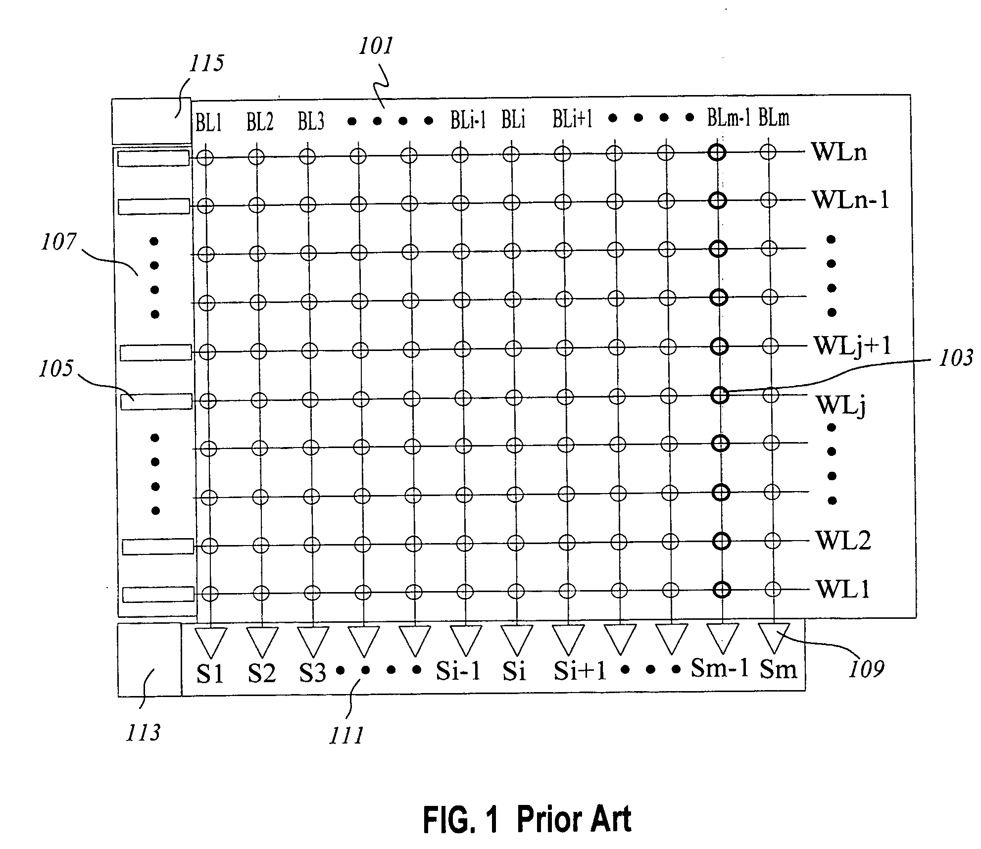
[0052] To access a set of data in the memory, the memory address is separated into three sub-sets to the decoders in three levels and decoded simultaneously. One botto...


PUM


Abstract

High performance memory devices have been realized by applying an Evenly Scaled Multiple Level Architecture (ESMLA) using block select arrangement. A single-bit-line-write mechanism allows us to reduce the number of bit lines by 50% for static memory devices. The resulting memory device can be as fast as registers files while its area is smaller than prior art high-density memory devices. The scaling method of the memory architecture also assures that the speed of the memory devices will scale in the same rate as logic circuits in future IC manufacture technologies.

Description

[0001] This is a Continuous-Prosecution-Application (CPA) of a co-pending application with Ser. No. 10 / 442,016 filed on May 19, 2003, and application Ser. No. 10 / 442,016 is a Divisional patent application of application Ser. No. 09 / 938,431 filed on Aug. 23, 2001 filed by the Applicant of this invention now issued on Aug. 12, 2003 into U.S. Pat. No. 6,606,275.FIELD OF THE INVENTION [0002] The present invention relates to high performance semiconductor-memory devices, and more particularly to memory devices having multiple level architecture. BACKGROUND OF THE INVENTION [0003] Memory devices and logic circuits are two major types of circuit components used in integrated circuits (IC). As IC manufacture technologies progress, both the density and the performance of logic circuits have been improved exponentially. Current art logic circuits are operating at multiple GHZ (billion cycles per second), while each chip can have more than 100 million gates. The density of IC memory devices is...

Claims


Application Information

Patent Timeline
Patent Type & Authority Applications(United States)
IPC IPC(8): G11C7/06G11C8/12
CPCG11C8/12G11C7/06
Inventor SHAU, JENG-JYE
Owner SHAU JENG JYE
Why Eureka
Try Eureka