NAND flash memory cell row and manufacturing method thereof

a memory cell and row technology, applied in the field of flash memory devices, can solve the problems of reducing the gate coupling ratio and the performance of the memory device, reducing the junction area of the conventional control gate and floating gate, and increasing the complexity of the writing and loading procedure of the memory cell of the nand array structure, so as to enhance the performance of the memory cell

Active Publication Date: 2006-02-23
POWERCHIP SEMICON MFG CORP
View PDF1 Cites 15 Cited by
  • Summary
  • Abstract
  • Description
  • Claims
  • Application Information

AI Technical Summary

Benefits of technology

[0010] Accordingly, one object of the present invention is to provide a NAND flash memory cell row to enhance the performance of a memory cell.

Problems solved by technology

However, when the size of the integrated circuit device is minimized, the junction area of the conventional control gate and floating gate is also reduced; thus, the gate coupling ratio and the performance of the memory device is reduced.
However, the writing and the loading procedure of the memory cell of the NAND array structure is more complex.
Therefore, the tunnel oxide layer will be damaged under high voltage operation and the stability will be reduced.

Method used


Image

  • NAND flash memory cell row and manufacturing method thereof
  • NAND flash memory cell row and manufacturing method thereof
  • NAND flash memory cell row and manufacturing method thereof

Examples


Embodiment Construction

[0020] The present invention now will be described more fully hereinafter with reference to the accompanying drawings, in which preferred embodiments of the invention are shown. This invention may, however, be embodied in many different forms and should not be construed as limited to the embodiments set forth herein; rather, these embodiments are provided so that this disclosure will be thorough and complete, and will fully convey the scope of the invention to those skilled in the art. Like numbers refer to like elements throughout.

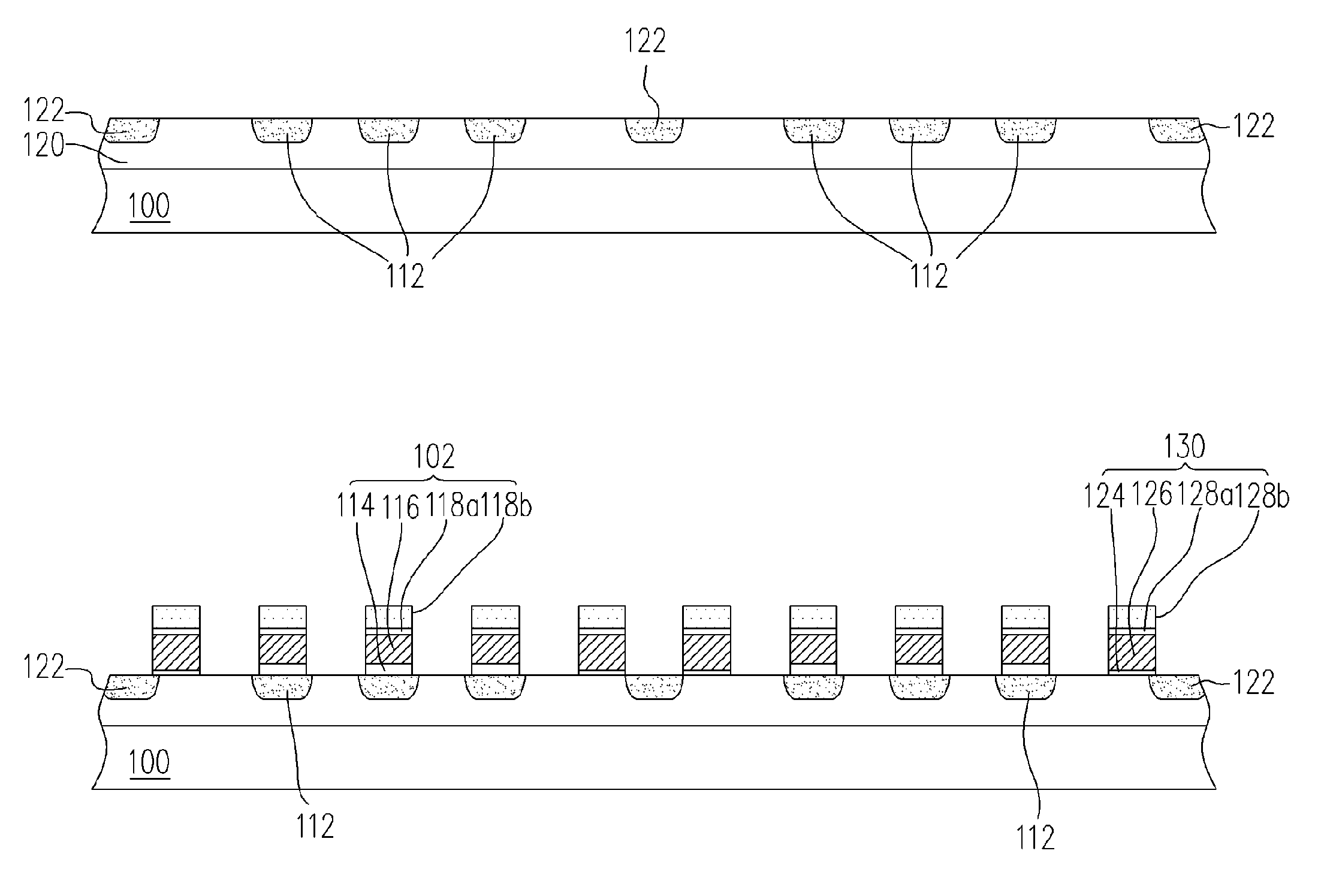
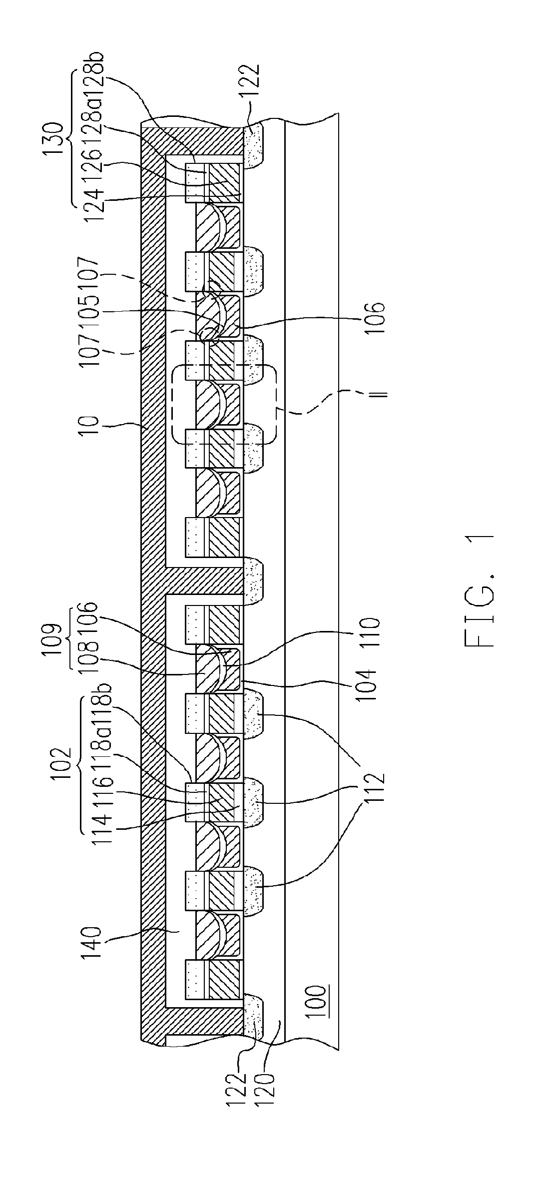
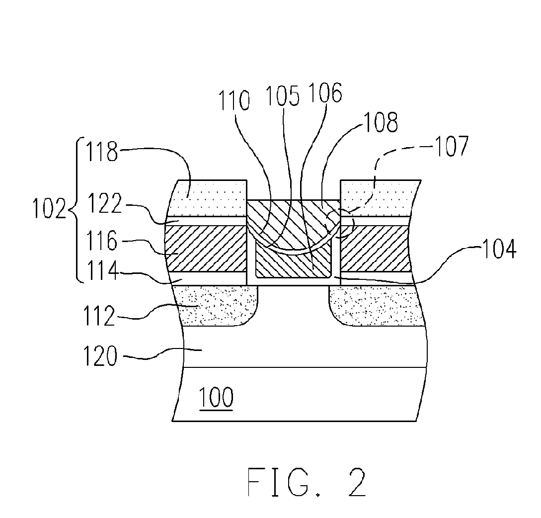
[0021]FIG. 1 is a cross-sectional view illustrating the structure of a NAND flash memory cell row according to the present invention. The memory cell rows illustrated in FIG. 1 have the same bit line 10, and each memory cell row has four memory cells. However, although the number of memory cells having the same bit line shown in FIG. 1 is only 4, the number of memory cells is not limited to 4. Instead, it is dependent on the design and requirement. For e...


PUM


Abstract

A NAND flash memory cell row includes first and second stacked gate structures, control and floating gates, inter-gate dielectric layer, a tunnel oxide layer, doping regions and source/drain regions. The first stacked gate structures has an erase gate dielectric layer, an erase gate and a first cap layer. Each of the second stacked gate structure has a select gate dielectric layer, a select gate and a second cap layer. The control gate is between each of the first stacked gate structures, and between each of the second stacked gate structures and the adjacent first stacked gate structure. The floating gate is between the control gate and substrate. The inter-gate dielectric layer is disposed between the control and floating gates. The tunnel oxide is between the floating gate and substrate. The doping regions are disposed under the first stacked gate structure, and the source/drain regions are in the exposed substrate.

Description

CROSS-REFERENCE TO RELATED APPLICATION [0001] This application is a divisional of a prior application Ser. No. 10 / 707,826, filed Jan. 15, 2004. All disclosures are incorporated herewith by reference.BACKGROUND OF THE INVENTION [0002] 1. Field of the Invention [0003] The present invention generally related to a flash memory device. More particularly, the present invention relates to a NAND flash memory cell row and the manufacturing method thereof. [0004] 2. Related Art of the Invention [0005] In recent years, flash memory device has become the main stream of the non-volatile memory device since that type of memory device allows for multiple data writing, loading and erasing operations. In addition, the stored data can be preserved even the power of the memory device is removed. [0006] In a conventional flash memory device, generally the floating gate and control gate of are manufactured with doped amorphous silicon. In a stacked gate flash memory device, the control gate is disposed...

Claims


Application Information

Patent Timeline
Patent Type & Authority Applications(United States)
IPC IPC(8): H01L21/8238
CPCH01L21/28273H01L27/115H01L27/11521H01L29/7887H01L29/42328H01L29/7881H01L29/42324H01L29/40114H10B69/00H10B41/30
Inventor CHEN, SHIH-CHANGHSU, CHENG-YUANHUNG, CHIH-WEI
Owner POWERCHIP SEMICON MFG CORP
Why Eureka
Try Eureka