
Optical sensor

a technology of optical sensors and optical sensors, applied in the field of optical sensors, can solve the problems of inability to properly detect the proportion of the detection object, and the absence or presence of the detection object, and achieve the effect of simple constitution and low cos

Active Publication Date: 2021-03-04
CANON KK
View PDF6 Cites 0 Cited by
  • Summary
  • Abstract
  • Description
  • Claims
  • Application Information

AI Technical Summary

Benefits of technology

The invention aims to create an optical sensor that can detect objects without being affected by direct light, and is cost-effective and easy to use.

Problems solved by technology

That is, the light receiving element is influenced by the light which directly enters the light receiving element through the gap, so that there was a problem such that portion of the detection object cannot be properly detected.
Further, in the case where the casing assembled later is replaced with the light guide made of the transparent resin material, the light guide is made of the transparent resin, and therefore, the light from the light emitting element directly enters the light receiving element, so that there was a problem such that presence or absence of the detection object cannot be properly detected.

Method used


Image

  • Optical sensor
  • Optical sensor
  • Optical sensor

Examples


embodiment 1

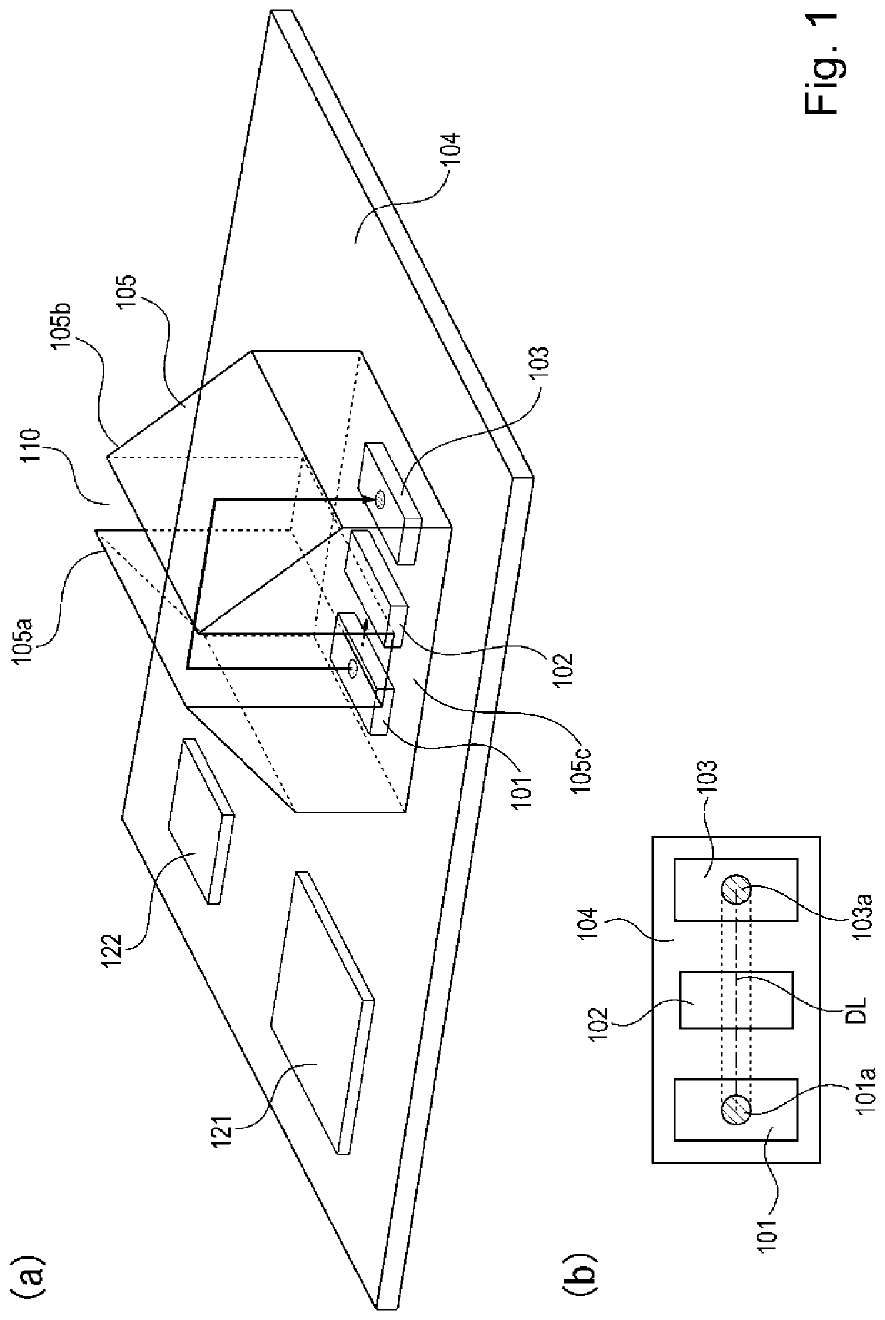
[0019]An optical sensor according to an embodiment 1 of the present invention will be described using FIG. 1. Part (a) of FIG. 1 is a perspective view of the optical sensor in the embodiment 1, and part (b) of FIG. 1 is a top plan view of the optical sensor in the embodiment 1.

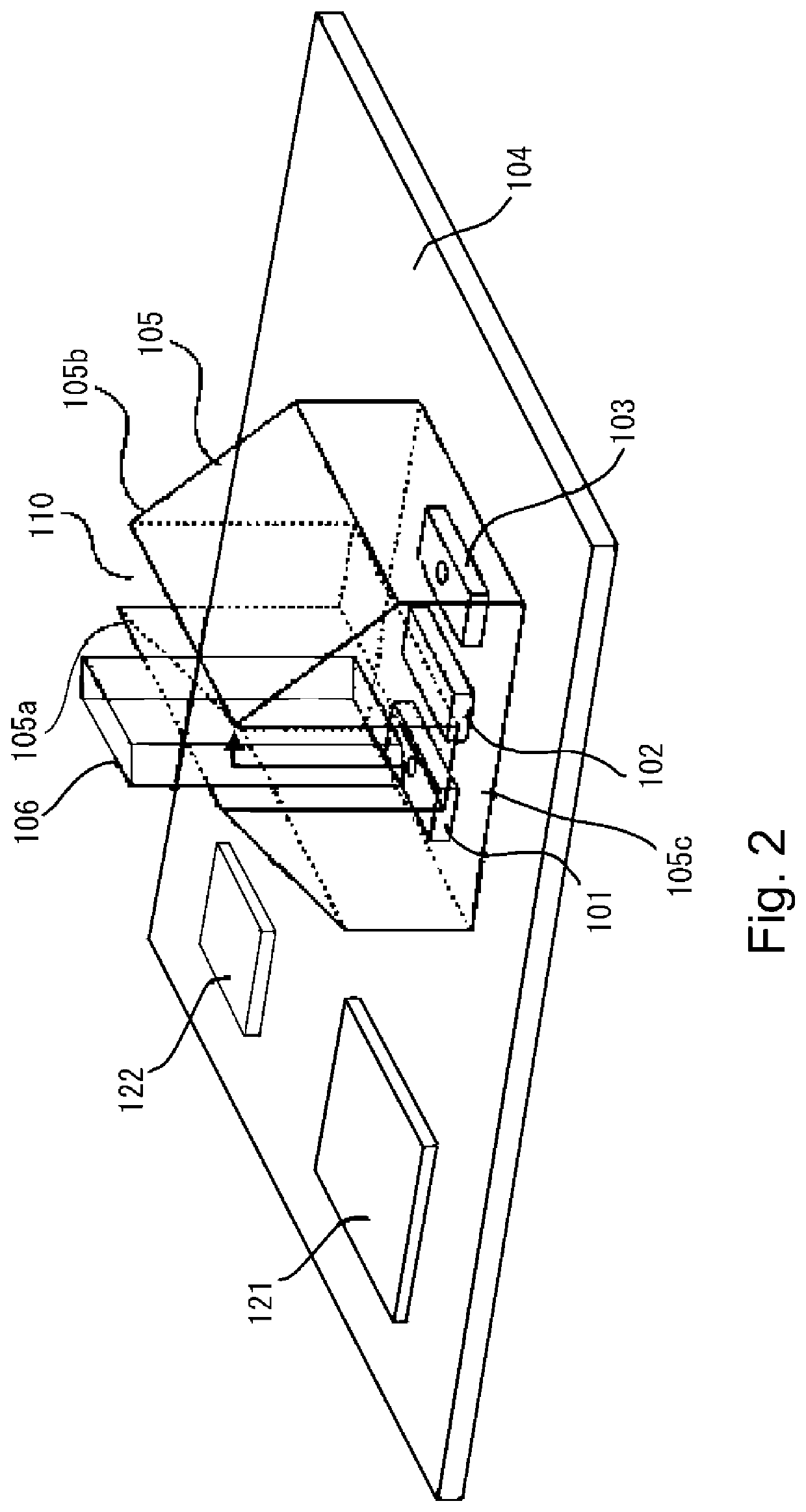
[0020]An optical sensor 100 according to the embodiment 1 includes a light emitting element 101 for emitting light, a light receiving element 103 for receiving the light from the light emitting element 101 through a space 110 in which a detection object (object to be detected) 106 (FIG. 2) passes, and an electronic circuit element 102. The optical sensor 100 detects the detection object 106 in such a manner that the light from the light emitting element 101 is blocked by the detection object 106 in the space 110 and thus an amount of the light received by the light receiving element 103 changes.

[0021]The light emitting element 101 includes a light emitting source 101a. In this embodiment, as the light emitting...

embodiment 2

[0048]An optical sensor according to an embodiment 2 of the present invention will be described with reference to FIGS. 6 and 7. In the embodiment 2, members (portions) similar to those in the embodiment 1 will be omitted from description. Part (a) of FIG. 6 is a perspective view of the optical sensor in this embodiment, and part (b) of FIG. 6 is a top plan view of the optical sensor in this embodiment. FIG. 7 is a schematic view showing a component part layout and a wiring pattern of the optical sensor in this embodiment.

[0049]An equivalent circuit of the optical sensor in this embodiment is the same in content as the equivalent circuit described in the embodiment 1 with reference to FIG. 4, and therefore will be omitted from description.

[0050]In the embodiment 2, an electronic circuit element disposed between the light emitting element 101 and the light receiving element 103 is a part of component parts constituting a driving circuit for driving the light emitting element 101 or t...

embodiment 3

[0054]An optical sensor according to an embodiment 3 of the present invention will be described with reference to FIG. 8. In the embodiment 3, members (portions) similar to those in the embodiments 1 and 2 will be omitted from description. FIG. 8 is a sectional view of the optical sensor in this embodiment.

[0055]The optical sensor in the embodiment 3 is provided with a back casing 108 including reflecting surfaces 109a and 109b instead of the light guide which is the light guiding member assembled later with the substrate. In the following, this will be specifically described.

[0056]In this embodiment, on the same surface of the substrate 104, the light emitting element 101, the electronic circuit element 102 and the light receiving element 103 are mounted early, and the casing 108 is mounted on the substrate 104 later. The black casing 108 is a member prepared by integrally forming a first hollow portion 108a including a first reflecting surface 109a, a second hollow portion 108b in...


PUM

PropertyMeasurementUnit
rated currentaaaaaaaaaa
voltageaaaaaaaaaa
currentaaaaaaaaaa

Abstract

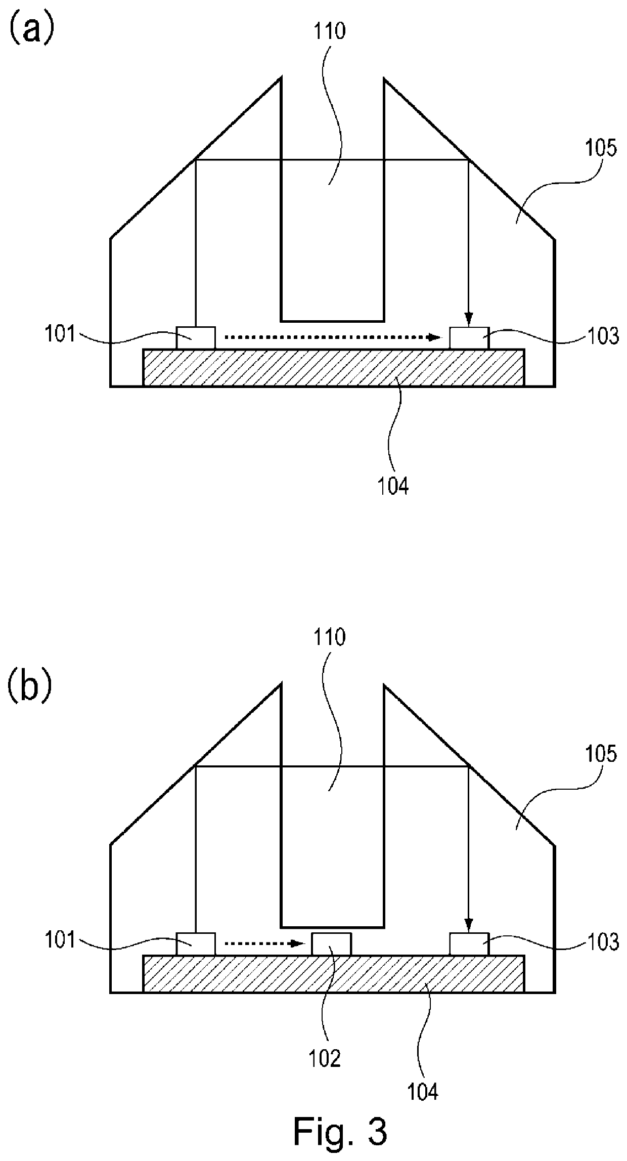
An optical sensor includes a substrate, a light emitting element, a light receiving element, and an electronic circuit element. Light from the light emitting element is blocked by a detection object to detect the detection object. The light emitting element, the electronic circuit element and the light receiving element are mounted on the same surface of the substrate. The electronic circuit element is disposed between the light emitting element and the light receiving element on a mounting surface of the substrate.

Description

FIELD OF THE INVENTION AND RELATED ART[0001]The present invention relates to an optical sensor for detecting a detection object (object to be detected) by using a light emitting element and a light receiving element.[0002]A transmitting type photo-interrupter as a conventional optical sensor uses the light emitting element such as an LED and the light receiving element such as a phototransistor and detects that light is blocked when the detection object passes through between the light emitting element and the light receiving element, so that detection of the detection object is carried out.[0003]For example, in the transmitting type photo-interrupter, a light emitting element of a surface mounting type and a light receiving element of a surface mounting type are mounted on the same surface of a substrate, and a casing including inner reflecting surfaces is assembled with the substrate on which these elements are mounted (Japanese Laid-Open Patent Application (JP-A) Hei 11-274550). ...

Claims


Application Information

Patent Timeline
Patent Type & Authority Applications(United States)
IPC IPC(8): G01V8/12
CPCG01V8/12G01V8/10H01L25/167H01L31/02325
Inventor TANAKA, SHUNSUKESUGIYAMA, NORIKAZU
Owner CANON KK
Learn More