Multilayer ceramic electronic component and method for manufacturing the same

a technology of multi-layer ceramics and electronic components, applied in the manufacture of capacitors, fixed capacitor details, fixed capacitors, etc., can solve the problems of difficult formation of side gaps between one side surface and the other side surface, and achieve the effect of less likely to be damaged or destroyed

Active Publication Date: 2021-03-25
MURATA MFG CO LTD
View PDF6 Cites 0 Cited by
  • Summary
  • Abstract
  • Description
  • Claims
  • Application Information

AI Technical Summary

Benefits of technology

[0019]The multilayer ceramic electronic components according to preferred embodiments of the present invention that each include a side surface with a side gap are each able to be less likely to be damaged or destroye

Problems solved by technology

In the method for forming a side gap described in Japanese Patent Laid-Open No. 2017-188559, however, a thin multilayer chip having dimension T smaller than dimension

Method used


Image

  • Multilayer ceramic electronic component and method for manufacturing the same
  • Multilayer ceramic electronic component and method for manufacturing the same
  • Multilayer ceramic electronic component and method for manufacturing the same

Examples


Embodiment Construction

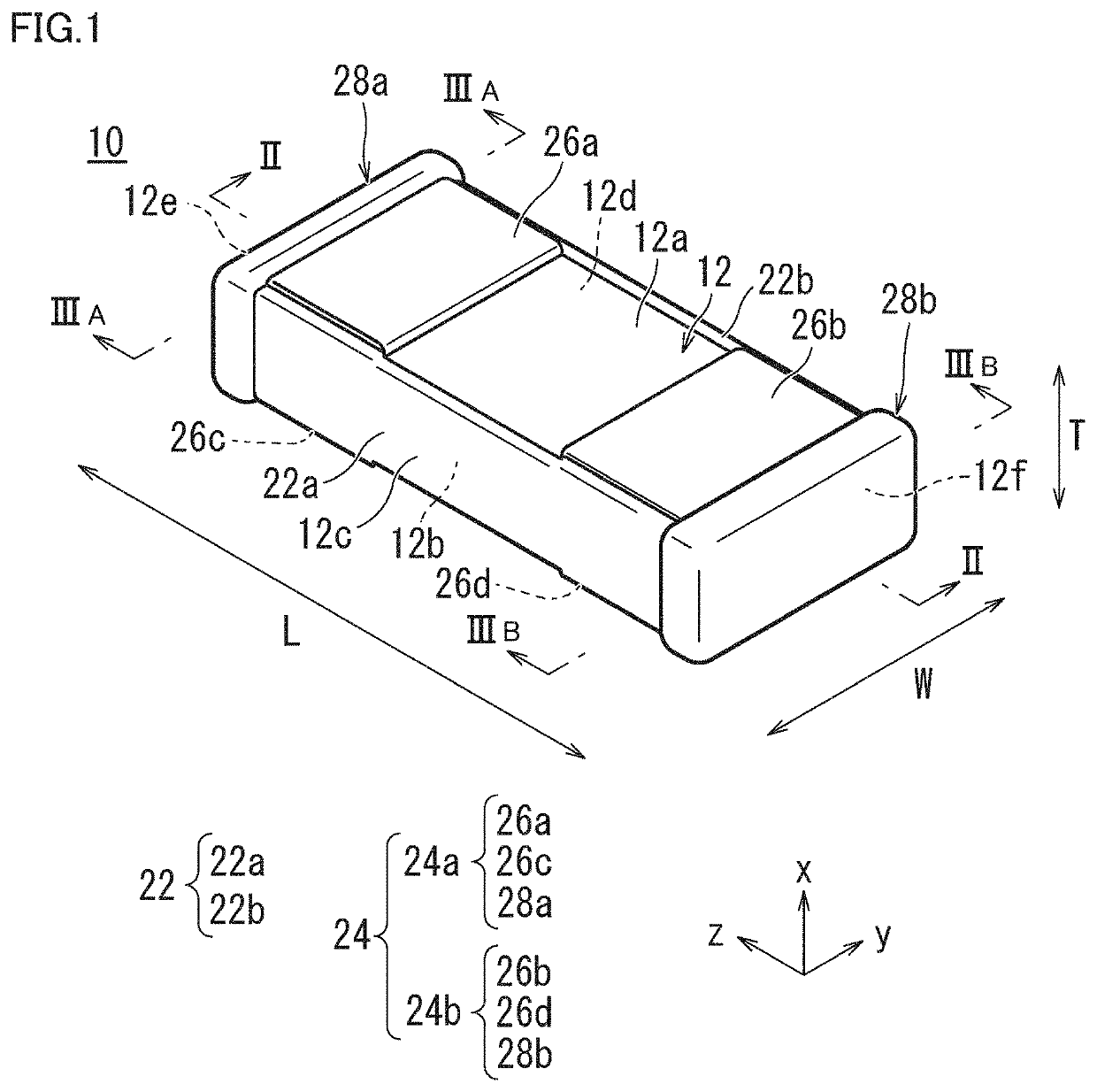
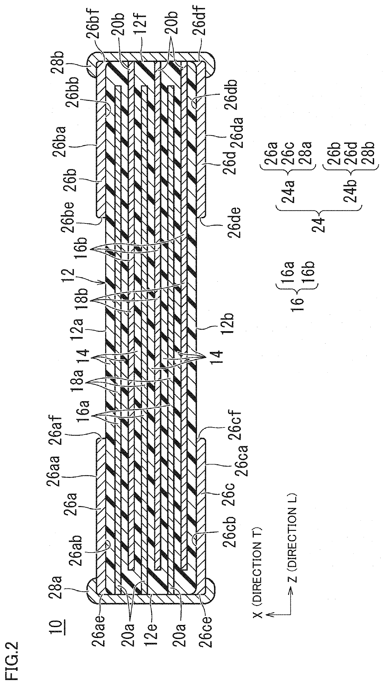
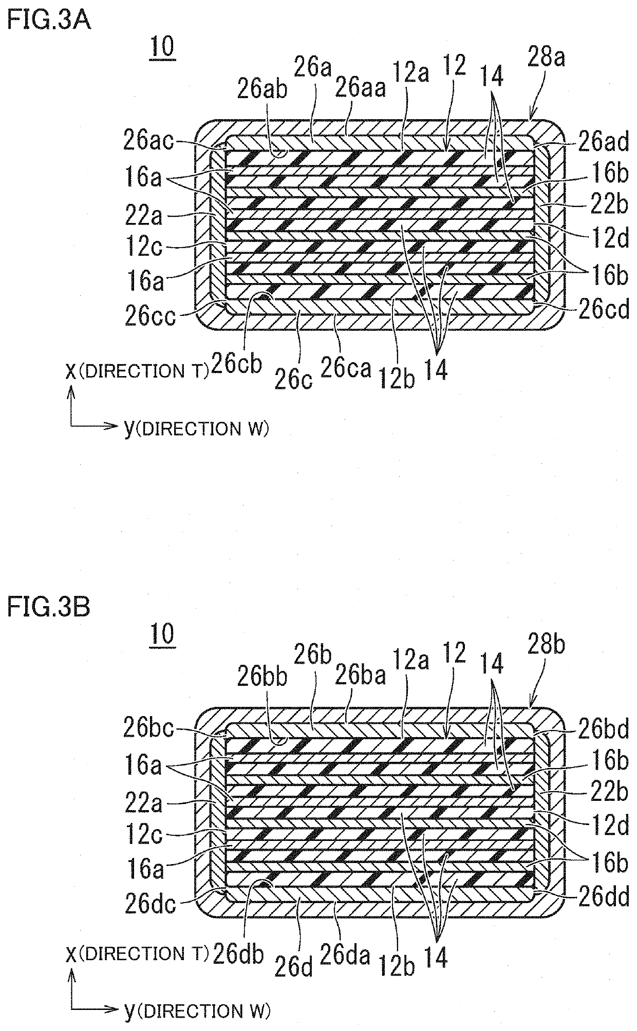
[0047]A multilayer ceramic capacitor as an example of a multilayer ceramic electronic component according to a preferred embodiment of the present invention will be described.

[0048]Specifically, a multilayer ceramic capacitor 10 according to the present preferred embodiment is a thin multilayer ceramic capacitor 10 having a dimension T smaller than a dimension W, as shown in FIGS. 1 to 3B.

[0049]Multilayer ceramic capacitor 10 manufactured in a method for manufacturing multilayer ceramic capacitor 10 according to the present preferred embodiment of the present invention will be described. FIG. 1 is an external perspective view showing an example of multilayer ceramic capacitor 10. FIG. 2 is a cross section taken along line II-II of FIG. 1 showing multilayer ceramic capacitor 10. FIG. 3A is a cross section taken along line IIIA-IIIA of FIG. 1 showing multilayer ceramic capacitor 10, and FIG. 3B is a cross section taken along line IIIB-IIIB of FIG. 1 showing multilayer ceramic capacito...


PUM

PropertyMeasurementUnit
Angleaaaaaaaaaa
Lengthaaaaaaaaaa
Lengthaaaaaaaaaa

Abstract

A multilayer ceramic electronic component includes a multilayer body including two major surfaces opposite to each other in a layer stacking direction, two side surfaces opposite to each other in a widthwise direction orthogonal or substantially orthogonal to the layer stacking direction, and two end surfaces opposite to each other in a lengthwise direction orthogonal or substantially orthogonal to the layer stacking direction and the widthwise direction, and external electrodes provided on the two end surfaces. A method for manufacturing the multilayer ceramic capacitor component includes preparing a plurality of multilayer bodies, stacking the plurality of multilayer bodies via a binder, rotating the plurality of multilayer bodies by about 90° with the lengthwise direction defining and functioning as an axis of rotation, and providing a side gap portion; and removing the binder from the multilayer body provided with the side gap portion.

Description

CROSS REFERENCE TO RELATED APPLICATIONS[0001]This application claims the benefit of priority to Japanese Patent Application No. 2019-170411 filed on Sep. 19, 2019. The entire contents of this application are hereby incorporated herein by reference.BACKGROUND OF THE INVENTION1. Field of the Invention[0002]The present invention relates to a method for manufacturing a multilayer ceramic electronic component and the multilayer ceramic electronic component, and more specifically to a method for manufacturing a thin multilayer ceramic electronic component and the thin multilayer ceramic electronic component.2. Description of the Related Art[0003]A multilayer ceramic capacitor is one type of multilayer ceramic electronic component. Such a multilayer ceramic capacitor includes a multilayer body and an external electrode. The multilayer body has a first major surface at one major surface, a second major surface at the other major surface, a first side surface at one side surface, a second si...

Claims


Application Information

Patent Timeline
IPC IPC(8): H01G4/30H01G4/248H01G13/00H01G4/232
CPCH01G4/30H01G4/232H01G13/006H01G4/248H01G4/12H01G4/252H01G13/06H01G4/1209
Inventor YOKOTA, YUSUKEMATSUI, TOGO
Owner MURATA MFG CO LTD
Why Eureka
Try Eureka