Integrated broadband ceramic capacitor array

a ceramic capacitor and broadband technology, applied in the field of miniature monolithic capacitors, can solve the problems of inability to avoid the relationship between capacitors used in electronic circuits and lumped elements cannot be readily realized in monolithic integrated circuits, and the inability to achieve equivalent series resistance and inductance. the effect of wideband performance, cost-effectiveness and superior performan

Inactive Publication Date: 2005-11-29
DEVOE DANIEL +2
View PDF16 Cites 54 Cited by
  • Summary
  • Abstract
  • Description
  • Claims
  • Application Information

AI Technical Summary

Benefits of technology

[0018]The present invention provides a capacitor having an effective wideband performance in an integrated, cost-effective structure. The capacitor of the present invention is an integrated array of capacitors connected in series and / or parallel circuits in a substantially monolithic dielectric body. The composition of the integrated capacitor array can be varied in order to tune the wideband capacitor to a particular application. Further, the integrated capacitor array of the present invention provides superior performance by providing less insertion loss than combinations of discrete capacitors. In addition, the wideband capacitor of the present invention is smaller and easier to handle and mount on a circuit board than combinations of discrete capacitors.

Problems solved by technology

Where part or all of the circuit is an analog circuit, such as a radio frequency transmitter or receiver, audio amplifier, or other such circuit, circuit design requires lumped elements that cannot be readily realized in monolithic integrated circuits.
Unfortunately, particularly at high frequencies, capacitors used in electronic circuits deviate substantially from this ideal relationship.
Accordingly, equivalent series resistance and inductance are not avoidable, and electronic design must take them into account, particularly in high frequency products such as broadband receiver / transmitters, short wave devices, and the like.
The resulting equivalent capacitance value is relatively large for the device size, albeit subject to imperfections due to resistance in the many current-carrying conductive structures, and inductance resulting from many plates carrying currents flowing in opposite directions.
While parallel capacitor combinations such as shown in FIGS. 8A and 8B have been used with some success in commercial devices, these combinations suffer from a number of drawbacks.
First, the measured capacitance of these parallel combinations exhibit variations (resonances and dropouts), likely due to a mismatch between the resonances of the effective L-R-C circuits that are created by the parallel connected capacitors.
Furthermore, the upper frequency response of even these parallel combinations may not meet the requirements of very wide band (GHz) devices in current use.
Also, the mechanical stacking of dual ceramic capacitors in the manner shown is not easily compatible with “tape and reel” assembly methods and thus, are cumbersome and expensive to implement in mass production.

Method used


Image

  • Integrated broadband ceramic capacitor array
  • Integrated broadband ceramic capacitor array
  • Integrated broadband ceramic capacitor array

Examples


Embodiment Construction

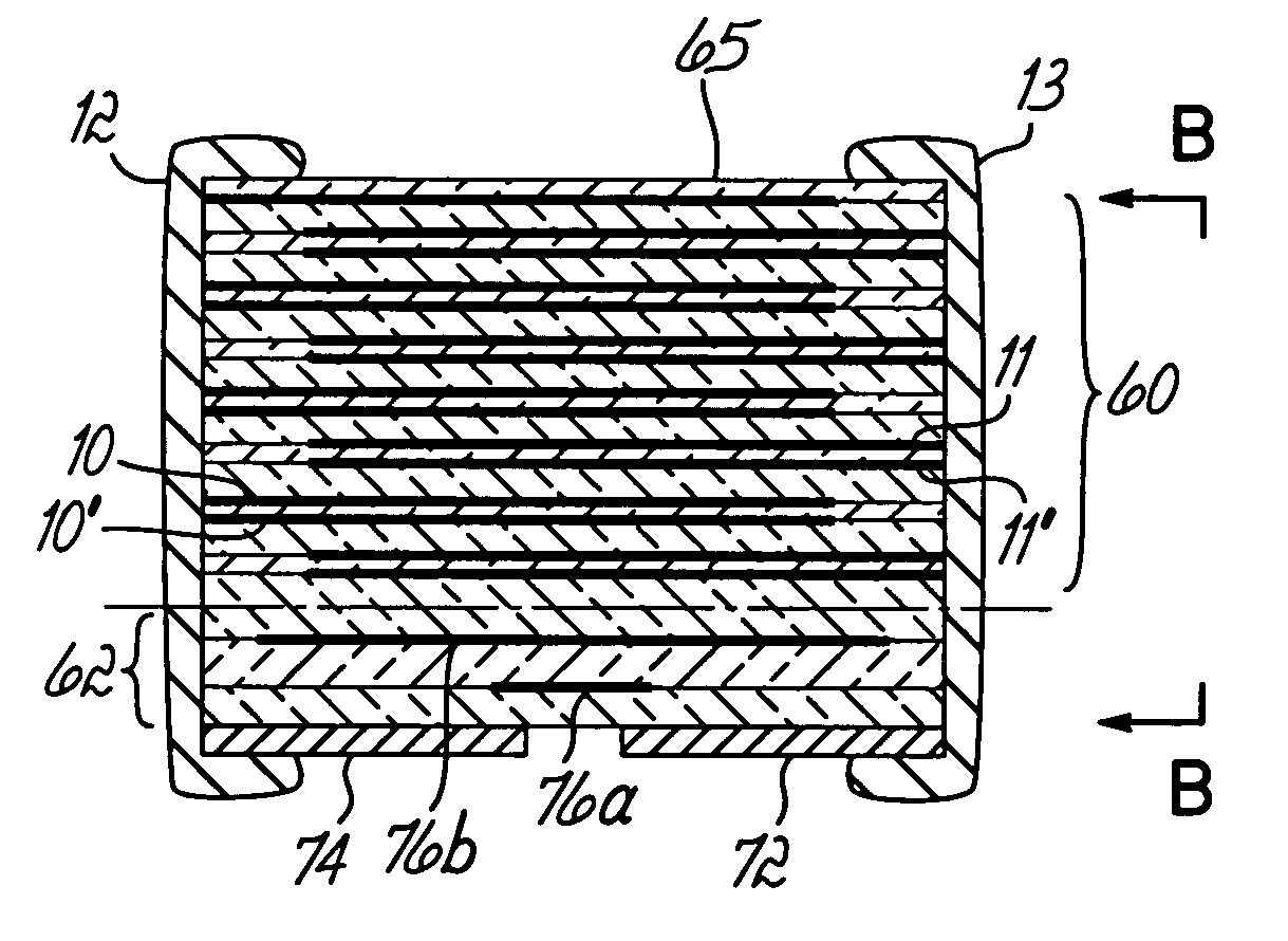
[0048]Referring now to FIG. 9A, a first embodiment of an integrated capacitor in accordance with certain aspects of the invention, can be described. In this embodiment, an integrated multi-layer and high frequency capacitor includes an upper section 60 including a multi-layer structure similar to that discussed above with reference to FIG. 2A, including plates 10 and 11 extending from conductive contacts 12 and 13, respectively, on opposite sides of a ceramic dielectric body. In this embodiment, individual plates extend from each side contact, rather than pairs of plates as shown in FIG. 2A. Using single plates in this manner increases the series inductance and resistance, for the reason that more current is caused to flow over each individual plate; however, more plates can be included in the capacitor using single plates, allowing an increase in capacitance value. Thus, the decision to use single or multiple plates is a tradeoff between capacitance and series resistance and induct...


PUM


Abstract

A monolithic capacitor structure includes opposed and overlapping plates within a dielectric body, which are arranged to form a lower frequency, higher value capacitor. Other conductive structure is located either inside the dielectric body or on an external surface thereof and is effective to form a higher frequency, lower value capacitor in parallel with the lower frequency, higher value capacitor. The resulting array of combined series and parallel capacitors integral with the dielectric body provides effective wideband performance in an integrated, cost-effective structure.

Description

[0001]This application is a continuation-in-part of U.S. application Ser. No. 10 / 412,992, filed Apr. 14, 2003, now U.S. Pat. No. 6,816,356 which, in turn, is a continuation-in-part of U.S. application Ser. No. 10 / 150,202, filed May 17, 2002, now U.S. Pat. No. 6,587,327.FIELD OF THE INVENTION[0002]The present invention relates to miniature monolithic capacitors.BACKGROUND OF THE INVENTION[0003]The development of integrated circuits has made it possible to place many circuit elements in a single semiconductor chip. Where part or all of the circuit is an analog circuit, such as a radio frequency transmitter or receiver, audio amplifier, or other such circuit, circuit design requires lumped elements that cannot be readily realized in monolithic integrated circuits. Capacitors in particular are frequently created as separate elements from the integrated circuit. The electronic device thus typically includes monolithic integrated circuits combined with external capacitors.[0004]For such a...

Claims


Application Information

Patent Timeline
Patent Type & Authority Patents(United States)
IPC IPC(8): H01G2/20H01G4/005H01G4/06H01G4/228H01G4/232H01G4/30H01G4/32H01G4/38H01G4/40H01G9/042H01G9/045
CPCH01G4/228H01G4/232H01G4/30H01G4/38H01G4/40
Inventor DEVOE, DANIELDEVOE, ALANDEVOE, LAMBERT
Owner DEVOE DANIEL
Why Eureka
Try Eureka