
Expansion electronic device and electronic system

a technology of electronic devices and expansion devices, applied in the field of laptop computers, can solve the problems of lack of waterproofness design of current laptop computers, compromised functionality of original laptop computers, etc., and achieve the effect of improving waterproofness and dustproofness, and enhancing the functionality of primary electronic devices

Active Publication Date: 2021-03-25
GETAC TECH CORP
View PDF0 Cites 4 Cited by
  • Summary
  • Abstract
  • Description
  • Claims
  • Application Information

AI Technical Summary

Benefits of technology

The present invention allows for a secondary device that can enhance the functionality of a primary device, improve waterproofing and dustproofing. The patient text describes an expansion electronic device with a housing and multiple functional modules. The housing has an assembly surface for joining with the primary device and individual receiving chambers for the modules. Structural interference between the assembly surface and the primary device creates a first waterproof space, while the separate modules create a second waterproof space. This invention provides a flexible and customizable way to add extra functions to a primary device while keeping it waterproof and dustproof.

Problems solved by technology

However, also because structures of current laptop computers are designed towards goals of being small in volume, light in weight and readily portable, functionality of original laptop computers is compromised.
In addition, current laptop computers lack designs for waterproofness.

Method used


Image

  • Expansion electronic device and electronic system
  • Expansion electronic device and electronic system
  • Expansion electronic device and electronic system

Examples


first embodiment

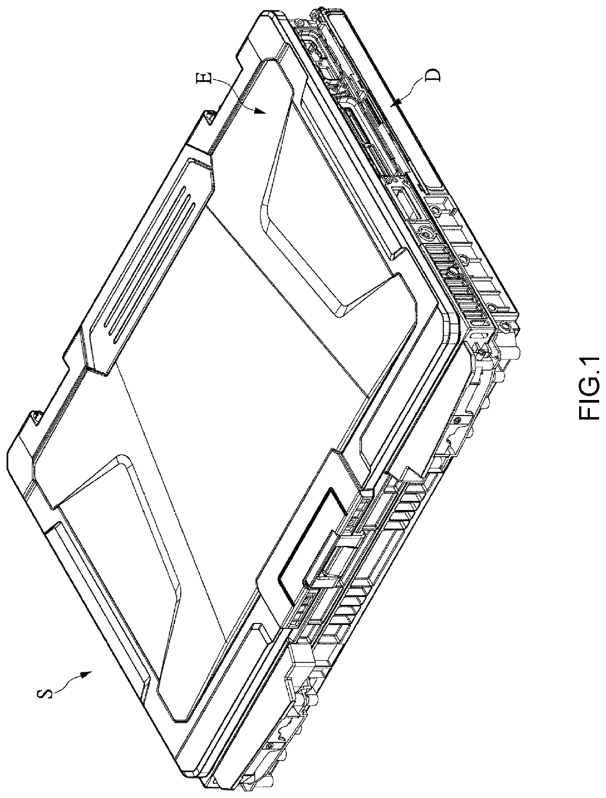
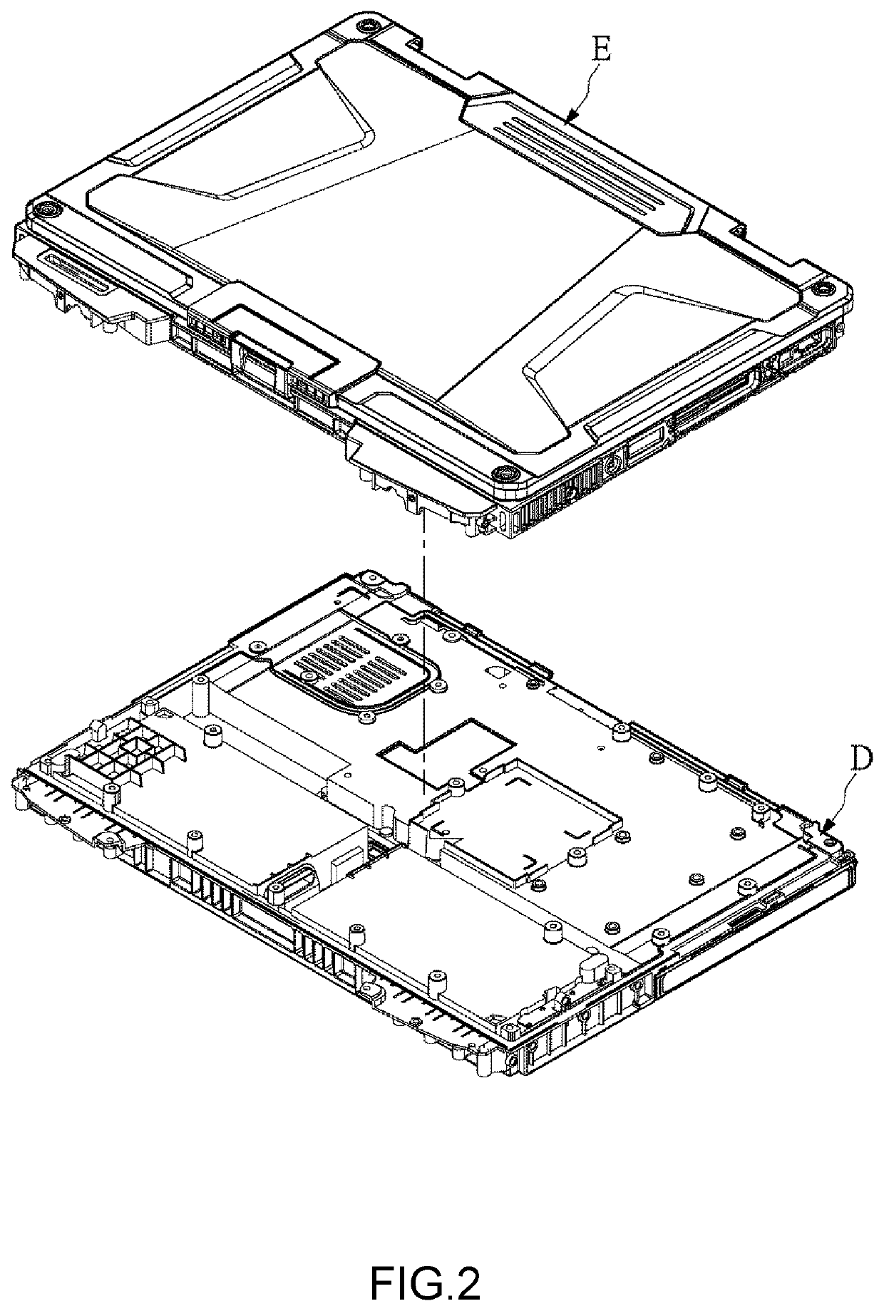
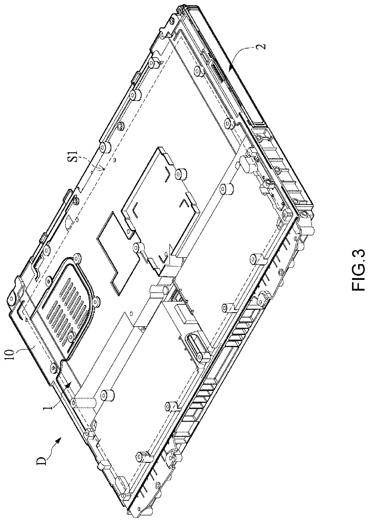
[0024]FIG. 1 to FIG. 4 are respectively a three-dimensional schematic diagram of an electronic system, an exploded schematic diagram of an electronic system, a three-dimensional schematic diagram of an expansion electronic device, and an exploded schematic diagram of an expansion electronic device according to a first embodiment of the present invention. As shown, an expansion electronic device D, adapted to be joined with a primary electronic device E and to operate cooperatively, is provided according to the first embodiment of the present invention. The expansion electronic device D may include a housing 1 and a plurality of functional modules 2 and 2a. The housing 1 may have an assembly surface 10 on a top side thereof, and a plurality of individually independent receiving chambers 11 and 11a on a bottom side thereof. The assembly surface 10 is configured to join with the primary electronic device E, and a first waterproof space S1 is formed by means of structural interference b...

second embodiment

[0029]FIG. 5 and FIG. 6 show a three-dimensional schematic diagram of an expansion electronic device and a three-dimensional schematic diagram of a primary electronic device according to a second embodiment of the present invention. Also refer to FIG. 1 to FIG. 4. As shown, the expansion electronic device D of this embodiment is substantially similar to the expansion electronic device D of the first embodiment, and repeated details are omitted herein. This embodiment differs from the first embodiment in that, in this embodiment, the assembly surface 10 has a central region 100 corresponding to the first waterproof space S1 and a border region 101 encircling the central region 100, and a first interference structure 1010 is provided in the border region 101; a second interference structure E1 configured to generate sealed interference with the first interference structure 1010 is provided on the bottom of the primary electronic device E. The first interference structure 1010 and the ...

third embodiment

[0032]FIG. 7 shows an exploded schematic diagram of an expansion electronic device according to a third embodiment of the present invention. Also refer to FIG. 1 to FIG. 6. As shown, the expansion electronic device D of this embodiment is substantially similar to the expansion electronic device D of the foregoing embodiments, and repeated details are omitted herein. This embodiment differs from the previous embodiments in that, in this embodiment, one of the receiving chambers 11a is provided therein with an enclosed block wall 110 configured to define the second waterproof space S2, and the enclosed block wall 100 has a third interference structure 1100. One of the functional modules 2a may include a base 20, and a fourth interference structure 200 configured to generate sealed interference with the third interference structure 1100 is provided on the bottom of the base 20. The third interference structure 1100 and the fourth interference structure 200 are a limiting channel and an...


PUM


Abstract

The present invention discloses an expansion electronic system and an electronic system. The expansion electronic device is adapted to be joined with a primary electronic device into one integral and to operate cooperatively. The expansion electronic device includes a housing and a plurality of functional modules. The housing has an assembly surface on a top side thereof and a plurality of individually independent receiving chambers on a bottom side thereof. The assembly surface is configured to join with the primary electronic device, and a first waterproof space is formed by means of structural interference between the assembly surface and the primary electronic device. The plurality of functional modules are disposed in the plurality of receiving chambers, respectively, and are individually installed or removed. A second waterproof space is formed by means of structural interference between one of the receiving chambers and the corresponding functional module.

Description

CROSS-REFERENCE TO RELATED APPLICATIONS[0001]The present application claims the benefit of U.S. provisional Patent Application No. 62 / 904,967, filed on Sep. 24, 2019, the disclosure of which is hereby incorporated by reference herein in its entirety.BACKGROUND OF THE INVENTIONField of the Invention[0002]The present invention relates to the technical field of laptop computers, and more particularly to an expansion electronic device and an electronic system.Description of the Prior Art[0003]Accompanied by rapid technology development, computers are thoroughly infiltrated into daily lives of the general public, such that computers are omni-present and have become indispensable necessities of the modern life. Laptop computers feature advantages of being small in volume, light in weight and readily portable compared to desktop computers, and so sale volumes of laptop computers continue to gradually rise year to year.[0004]However, also because structures of current laptop computers are d...

Claims


Application Information

Patent Timeline
Patent Type & Authority Applications(United States)
IPC IPC(8): H05K5/06H05K5/02
CPCH05K5/069H05K5/0204H05K5/061H01Q1/2266H01Q21/08G06F1/1698E05Y2999/00G06F1/1656G06F1/1616H05K5/0017H05K5/04G06F1/1679G06F1/1683E05D3/02E05D5/04F16C11/04G06F1/1654
Inventor CHOU, HSIN-CHIHCHANG, JUEI-CHI
Owner GETAC TECH CORP
Learn More