Output circuit having voltage-withstanding mechanism

a technology of output circuit and resistance mechanism, which is applied in the direction of pulse technique, electronic switching, semiconductor devices, etc., can solve the problems of unstable voltage of voltage source, inability to operate, and easy damage of components, so as to achieve the effect of preventing voltage source from operating in an unstable condition

Active Publication Date: 2021-04-01
REALTEK SEMICON CORP
View PDF0 Cites 0 Cited by
  • Summary
  • Abstract
  • Description
  • Claims
  • Application Information

AI Technical Summary

Benefits of technology

[0005]The present disclosure discloses an output circuit having a voltage-withstanding mechanism that includes a PMOS transistor, a NMOS transistor, a voltage-withstanding auxiliary NMOS transistor and a voltage-withstanding auxiliary circuit. The PMOS transistor includes a first source terminal and a first drain terminal electrically coupled to a voltage source and an output terminal respectively and a first gate configured to receive a first input signal. The NMOS transistor includes a second source terminal and a second drain terminal electrically coupled to a ground terminal and a connection terminal respectively and a second gate configured to receive a second input signal. The voltage-withstanding auxiliary NMOS transistor includes a third drain terminal and a third source terminal

Problems solved by technology

However, in some operation environments, the voltage source may operate under an unstable condition such that the voltage thereof is too high.
Under such a situation, if an auxiliary circu

Method used


Image

  • Output circuit having voltage-withstanding mechanism
  • Output circuit having voltage-withstanding mechanism

Examples


Embodiment Construction

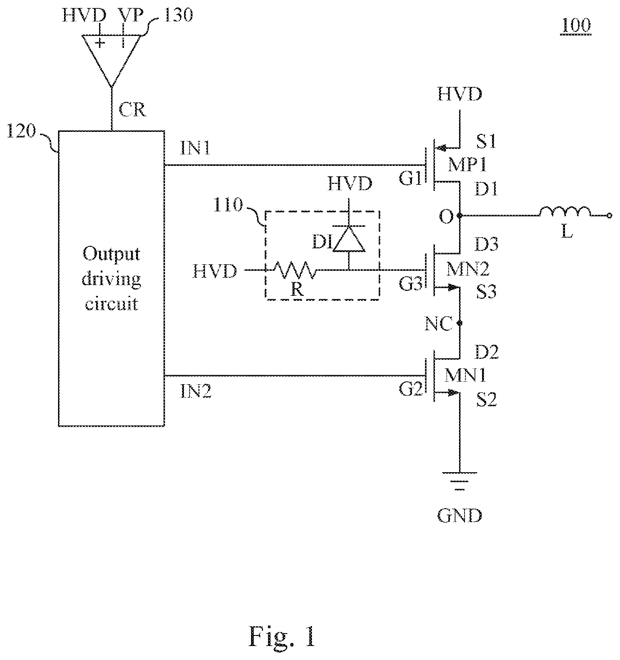
[0009]An aspect of the present invention is to provide an output circuit having a voltage-withstanding mechanism to increase the voltage-withstanding ability of the output circuit to further increase the reliability of the output circuit.

[0010]Reference is now made to FIG. 1. FIG. 1 illustrates a circuit diagram of an output circuit 100 having a voltage-withstanding mechanism according to an embodiment of the present invention. The output circuit 100 includes a PMOS transistor MP1, a NMOS transistor MN1, a voltage-withstanding auxiliary NMOS transistor MN2 and a voltage-withstanding auxiliary circuit 110.

[0011]The PMOS transistor MP1 includes a first source terminal 51 and a first drain terminal D1 electrically coupled to a voltage source HVD and an output terminal O respectively, and a first gate G1 configured to receive a first input signal IN1. The NMOS transistor MN1 includes a second source terminal S2 and a second drain terminal D2 electrically coupled to a ground terminal GND...


PUM


Abstract

The present disclosure discloses an output circuit having a voltage-withstanding mechanism that includes a PMOS, a NMOS, a voltage-withstanding auxiliary NMOS and a voltage-withstanding auxiliary circuit. The PMOS includes a first source terminal and a first drain terminal coupled to a voltage source and an output terminal and a first gate receiving a first input signal. The NMOS includes a second source terminal and a second drain terminal coupled to a ground terminal and a connection terminal and a second gate receiving a second input signal. The auxiliary NMOS includes a third drain terminal and a third source terminal coupled to the output terminal and the connection terminal The auxiliary circuit is coupled to the voltage source and a third gate of the auxiliary NMOS and provides a current conducting mechanism and a resistive mechanism respectively when the output terminal is operated at a logic high level and a logic low level.

Description

BACKGROUND OF THE INVENTION1. Field of the Invention[0001]The present disclosure relates to an output circuit having a voltage-withstanding mechanism.2. Description of Related Art[0002]In integrated circuit (IC) design, an output circuit is usually disposed as the last stage circuit of a circuit module such that a signal processed by the circuit module can be outputted to an external circuit module. Based on an amount of a voltage of a voltage source that the output circuit operates accordingly, components in the output circuit, e.g. PMOS transistors or NMOS transistors, need to have a reliable voltage-withstanding ability to withstand the voltage of the voltage source such that the components are able to operate in a reasonable range without being damaged.[0003]However, in some operation environments, the voltage source may operate under an unstable condition such that the voltage thereof is too high. Under such a situation, if an auxiliary circuit design that helps the components ...

Claims


Application Information

Patent Timeline
IPC IPC(8): H03K17/081
CPCH03K17/08104H03K17/08H03K17/08142
Inventor TSAUR, TAY-HERTSAI, TSUNG-YEN
Owner REALTEK SEMICON CORP
Why Eureka
Try Eureka