Electronic device and method of manufacturing the same
- Summary
- Abstract
- Description
- Claims
- Application Information
AI Technical Summary
Benefits of technology
Problems solved by technology
Method used
Image

Examples
Embodiment Construction
[0039]Like reference symbols in the various drawings indicate like elements unless otherwise indicated.
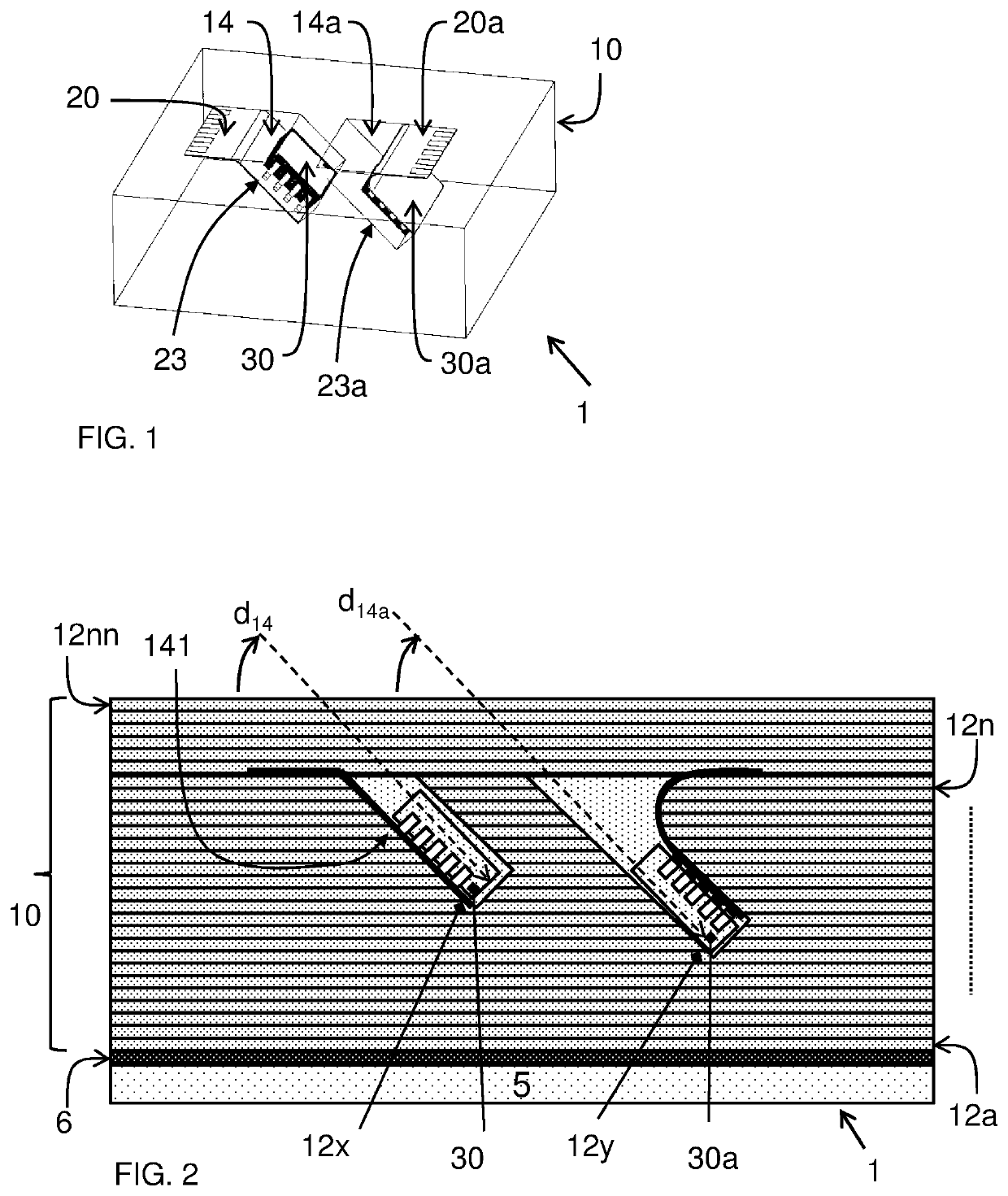
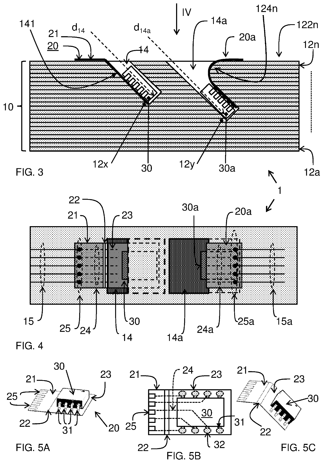
[0040]FIG. 1. shows an electronic device 1 that comprises a stack 10 of layers. The stack 10 has a cavity 14 wherein a component carrier 23, which is part of a carrier module 20 and provided with an electronic component 30 is arranged. The electronic product in this example comprises a further electronic component 30a which is arranged on a further component carrier 23a within a further cavity 14b in the stack 10.
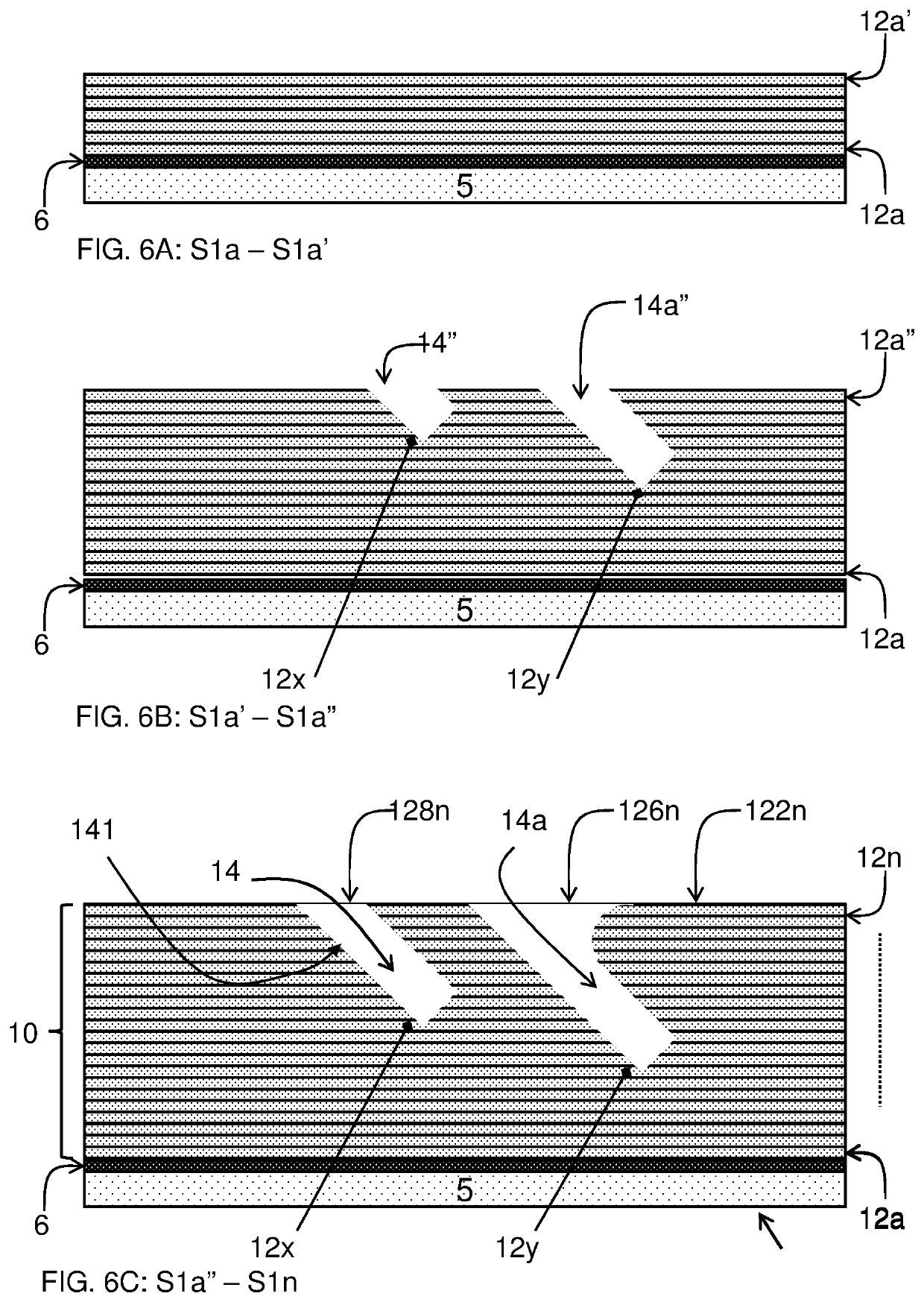
[0041]FIG. 2 shows a cross-sectional view of the product of FIG. 1. As shown therein, the cavity 14 extends through the stack of layers from one of the layers, denoted as 12n to another one of said layers 12x in a direction d14. The direction is d14 is in between a direction aligned with a plane of the one 12n of the layers and a direction perpendicular to that plane. In the example shown the direction of the cavity 14 is at an angle of approximately 45 degrees. Alternativ...
PUM
 Abstract
Description
Claims
Application Information