Radio frequency switch circuit, chip, and communication terminal

a radio frequency switch and circuit technology, applied in electronic switching, pulse technique, semiconductor devices, etc., can solve the problems of severe affecting the efficiency of antennas, deterioration of harmonics generated by single-pole multi-throw switches, severe affecting antenna tuning performance, etc., to improve the overall voltage withstanding ability of radio frequency switch circuits, improve the uniformity of voltage distribution on the switch chain, and reduce harmonics

Pending Publication Date: 2021-10-07
VANCHIP TIANJIN TECH
View PDF0 Cites 1 Cited by
  • Summary
  • Abstract
  • Description
  • Claims
  • Application Information

AI Technical Summary

Benefits of technology

[0020]Preferably, a third capacitor is disposed between a source and a body of an MOS transistor of each switch unit; and a ratio of a parasitic capacitance between MOS transistors to a capacitance of the third capacitor is adjusted, to improve voltage distribution uniformity on the switch chain when the radio frequency switch circuit is turned off.
[0021]Preferably, a size of the MOS transistor of the each switch unit and a ratio of the size to a size of the third capacitor are adjusted, to improve voltage distribution uniformity on the switch chain when the radio frequency switch circuit is turned off, where the size of the MOS transistor is a width / length (W / L) ratio of a gate of the MOS transistor.
[0027]In the radio frequency switch circuit provided in the present invention, a switch chain is formed by at least one switch unit disposed between the first port and the second port, each switch unit is connected to the first bias circuit and the second bias circuit, and the ratio of the parasitic capacitance between MOS transistors of the switch units to the capacitance of the third capacitor, the size of the MOS transistor of the each switch unit, and the ratio of the size to the size of the third capacitor are further adjusted. In this way, voltage distribution uniformity on the switch chain can be improved, thereby improving the overall voltage withstanding ability of the radio frequency switch circuit and reducing the occurrence of harmonics.

Problems solved by technology

In addition, with the thinning of smartphones and the increase of components, increasingly small space is left for antennas, which severely affects the efficiency of the antennas.
When a voltage withstood by the each switch unit is close to a rated breakdown voltage of the single-pole multi-throw switch, harmonics generated by the single-pole multi-throw switch deteriorate.
If the voltage is further increased and exceeds the breakdown voltage of the single-pole multi-throw switch, the harmonics rise in a cliff-like manner, severely affecting the antenna tuning performance.
When the voltage swing withstood by the switch is increased, a voltage withstood by each switch unit increases accordingly, causing the harmonics to deteriorate.

Method used


Image

  • Radio frequency switch circuit, chip, and communication terminal
  • Radio frequency switch circuit, chip, and communication terminal
  • Radio frequency switch circuit, chip, and communication terminal

Examples


embodiment 1

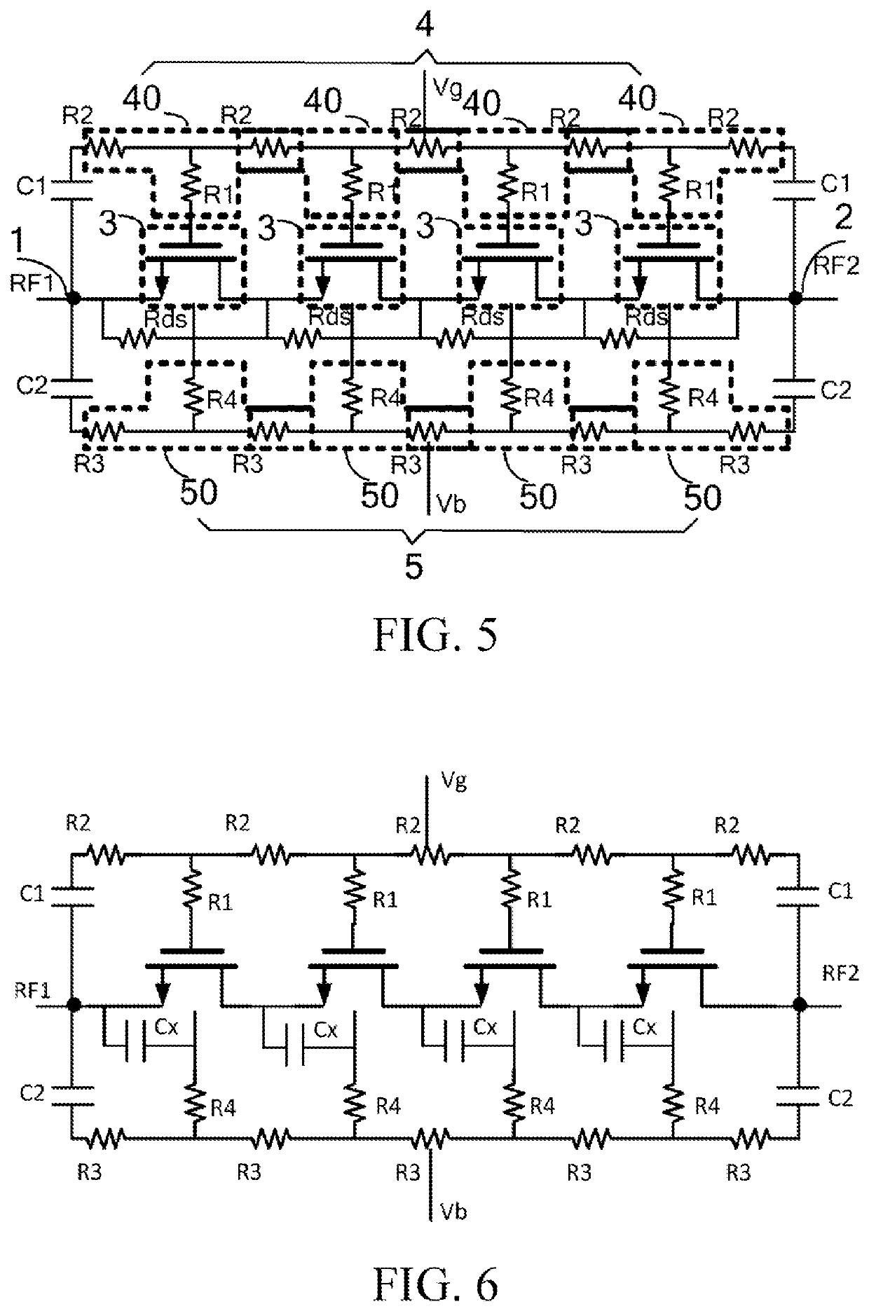
[0040]As shown in FIG. 5, a radio frequency switch circuit provided in Embodiment 1 includes a first port 1 and a second port 2. A switch chain is formed by at least one switch unit 3 between the first port 1 and the second port 2. Each switch unit 3 is connected to a first bias circuit 4 and to a second bias circuit 5, and bias voltages are connected at preset positions of the first bias circuit 4 and the second bias circuit 5.

[0041]When the switch chain includes one switch unit 3, an input end of the switch unit is used as an input end of the switch chain, and an output end of the switch unit is used as an output end of the switch chain. The input end of the switch unit 3 is connected to the first port 1, and the output end of the switch unit 3 is connected to the second port 2. Both the first port 1 and the second port 2 are used as input ports of a radio frequency signal, so that the radio frequency switch circuit is bidirectional. The radio frequency signal may be inputted from...

embodiment 2

[0053]As shown in FIG. 6, an example in which the switch units 3 respectively use NMOS transistors is used. Based on the radio frequency switch circuit provided in Embodiment 1, in a radio frequency switch circuit provided in this embodiment, a third capacitor Cx is disposed between the source and the body of the NMOS transistor of each of the switch units 3. The third capacitor Cx is used as a compensation capacitor of the switch unit 3. Alternatively, the third capacitor Cx may be disposed between the source and the gate of the NMOS transistor of each switch unit 3. The sizes of the NMOS transistors of the switch units may be different, and larger sizes of the NMOS transistors of the switch units 3 indicate larger parasitic capacitances. Therefore, a ratio of a parasitic capacitance between the NMOS transistors of the switch units 3 to a capacitance of the third capacitor Cx is adjusted, to further improve voltage distribution uniformity on the switch chain when the radio frequenc...

embodiment 3

[0054]As shown in FIG. 7, an example in which the switch units 3 respectively use NMOS transistors is used. Based on the radio frequency switch circuit provided in Embodiment 2, in a radio frequency switch circuit provided in this embodiment, the W / L ratio of the gate of the NMOS transistor of each switch unit 3 is further adjusted. Specifically, a voltage withstanding value of the NMOS transistor of each switch unit 3 is related to the length of the gate of the NMOS transistor. A larger length L of the gate of the NMOS transistor indicates a higher voltage withstanding value of the NMOS transistor, which is conducive to improving the voltage withstanding ability when the radio frequency switch circuit is turned off. However, when the NMOS transistor is turned on, the impedance of the NMOS transistor becomes higher, causing higher insertion loss. To maintain a proper insertion loss value, the width W of the radio frequency switch circuit may be increased. In this case, an overlap ca...


PUM


Abstract

Disclosed are a radio frequency switch circuit, a chip, and a communication terminal. In the radio frequency switch circuit, a switch chain is formed by at least one switch unit being provided between a first port and a second port; each switch unit is connected to a first bias circuit and to a second bias circuit; further adjustments are made to the ratio of the parasitic capacitance between MOS transistors of each switch unit to a third capacitance; and adjustments are made to the size of said MOS transistors as well as to the ratio of said size to the third capacitance. In this way, voltage distribution uniformity on the switch chain may be improved, thus increasing the overall voltage withstand ability of the radio frequency switch circuit, and reducing the occurrence of harmonic events.

Description

BACKGROUNDTechnical Field[0001]The present invention relates to a radio frequency switch circuit, and also to a corresponding integrated circuit chip and a communication terminal, belonging to the field of radio frequency circuit technologies.Related Art[0002]With the development of wireless communication technologies, communication standards have undergone the evolution of eras from 3G, 4G to 5G, and are developed from the early single standard covering several frequency bands to the current multi-standard covering a dozen or even dozens of frequency bands. To switch between different frequency bands and standards, it is necessary to use a radio frequency switch circuit. In addition, with the thinning of smartphones and the increase of components, increasingly small space is left for antennas, which severely affects the efficiency of the antennas. Therefore, a tuning switch is generally introduced to change an electrical length of an antenna, to improve the performance of the anten...

Claims


Application Information

Patent Timeline
Patent Type & Authority Applications(United States)
IPC IPC(8): H03K17/687
CPCH03K17/6874H04B1/40H03K17/102H03K17/08142H03K2217/0018Y02D30/70
Inventor LIN, SHENG
Owner VANCHIP TIANJIN TECH
Why Eureka
Try Eureka