
Touch panel and display device

a display device and touch panel technology, applied in the field of display devices, can solve the problems of inability to achieve the effect of reducing overlap of metal lines, avoiding widening of metal lines, and improving stacking position deviation

Active Publication Date: 2021-11-18
WUHAN CHINA STAR OPTOELECTRONICS SEMICON DISPLAY TECH CO LTD
View PDF0 Cites 0 Cited by
  • Summary
  • Abstract
  • Description
  • Claims
  • Application Information

AI Technical Summary

Benefits of technology

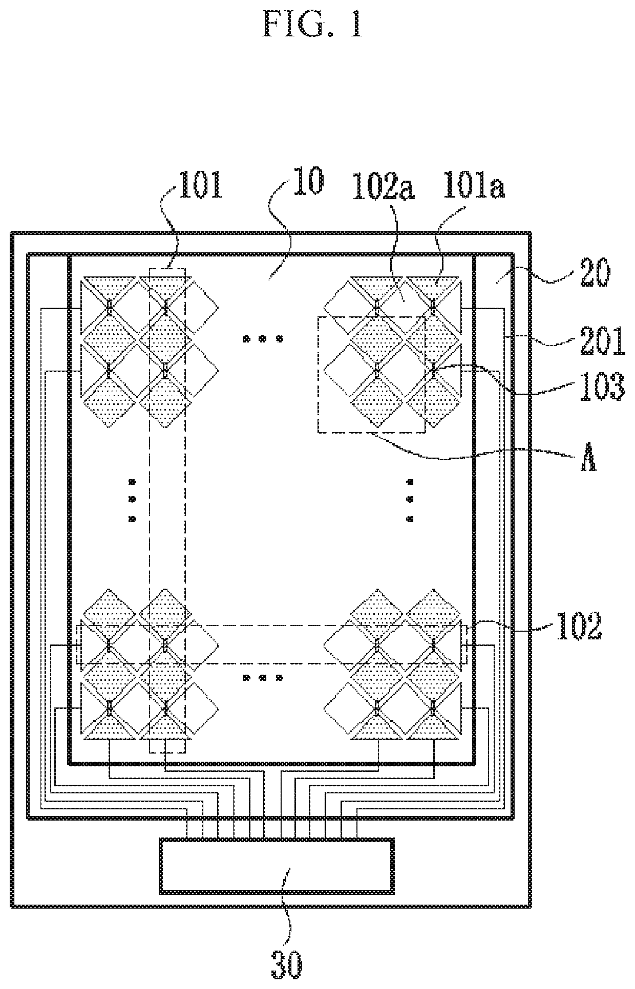
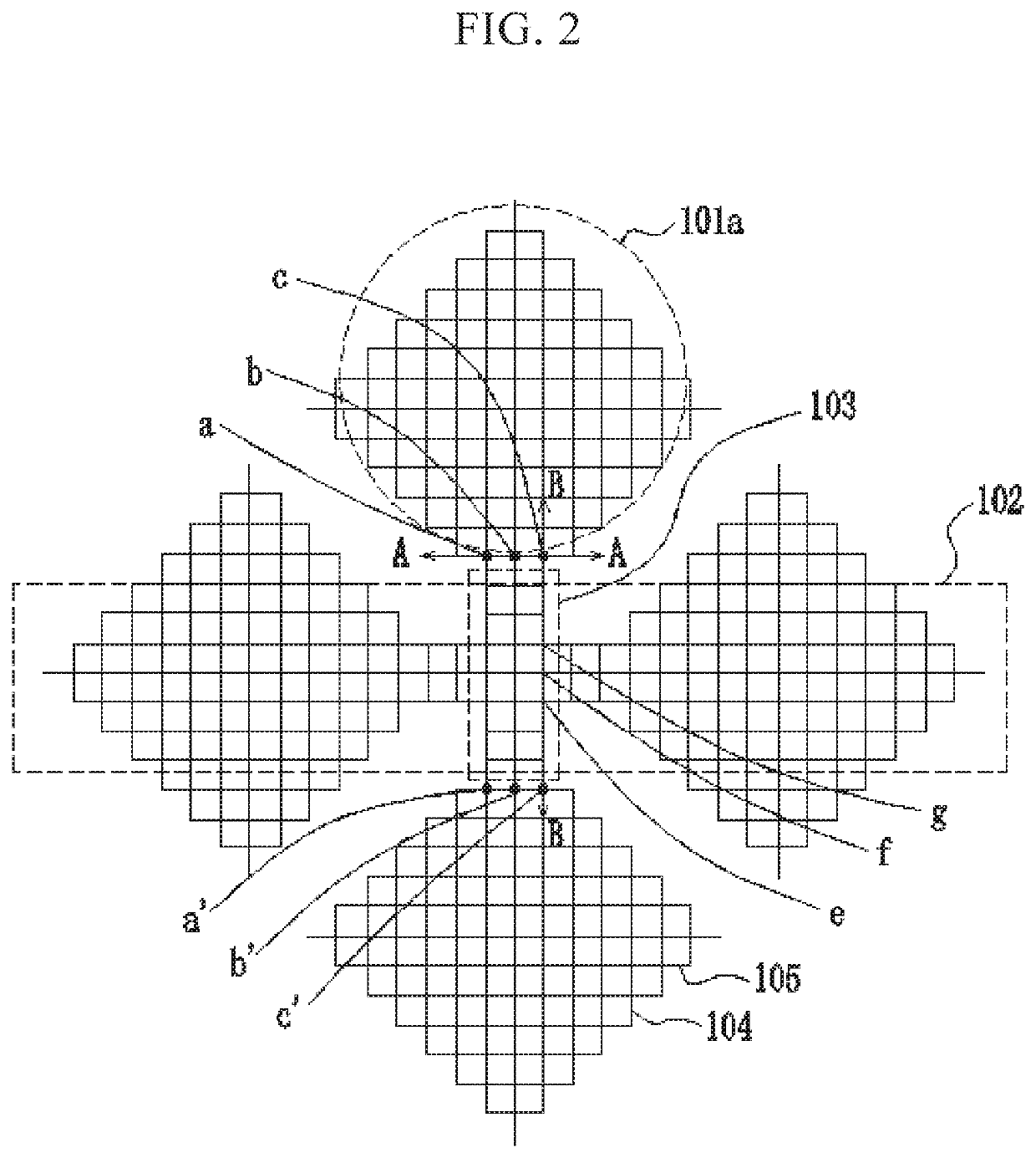
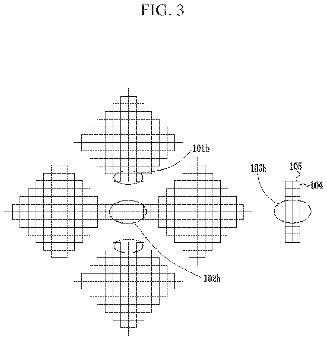
The present invention provides a touch panel and display device that can avoid optical defects or local moiré patterns caused by stacking position deviation between a bridging layer and an electrode pattern layer. The BRIDGING layer cooperates with the first and second electrode chains to reduce overlapping metal lines in directions vertical to the chains, and avoids widening of metal lines caused by alignment deviation between upper and lower layers. This improves the stacking position of the layers. The connection through the via holes is easy to achieve and has high precision in manufacturing processes.

Problems solved by technology

However, the metal mesh mutual-capacitive touch structures are often affected by bridging point connection manners.
Conditions in bridging point connection, such as poor linking or stacking position deviation, may cause bridging point connection lines to appear widened, which results in optical defects or even local moiré patterns.
Therefore, conventional techniques have drawbacks and are in urgent need of improvement.

Method used


Image

  • Touch panel and display device
  • Touch panel and display device
  • Touch panel and display device

Examples


Embodiment Construction

[0038]Embodiments of the present disclosure are described in detail with reference to the accompanying drawings as follows. Directional terms such as up / down, front / rear, right / left, inside / outside, and the like may be used for the purpose of enhancing a reader's understanding about the accompanying drawings, but are not intended to be limiting. Specifically, the terminologies in the embodiments of the present disclosure are merely for the purpose of describing certain embodiments, but not intended to limit the scope of the invention. The same reference numbers are used throughout the drawings to refer to the same or similar parts.

[0039]The present invention is directed to solving an existing problem in conventional touch panels. The problem is that the metal mesh-like bridging layer and the electrode layer may have a stacking position deviation, which causes connection lines of the bridging layer to appear to be widened, thereby causing optical defects and even local moiré patterns...


PUM


Abstract

The present invention provides a touch panel and a display device. The touch panel includes multiple first electrode chains and multiple second electrode chains. Each of the first electrode chains includes multiple first electrodes electrically connected through bridging layers. Each of the first electrodes, the bridging layers, and the second electrode chains consists of mesh metal lines. Each of the first electrode includes a first mesh metal line defect portion, and each of the second electrode chain includes multiple second mesh metal line defect portions. The bridging layers are complementary to the first mesh metal line defect portions and the second mesh metal line defect portions.

Description

1. FIELD OF DISCLOSURE[0001]The present invention relates to a field of display devices and in particular, to a touch panel and a display device.2. DESCRIPTION OF RELATED ART[0002]At present, touch panels generally include a carrier layer and a touch structure formed on the carrier layer, and touch positions are sensed by a capacitance change of the touch structure. With development of touch panels, metal mesh mutual-capacitive touch structures are increasingly used in production due to their excellent performance. However, the metal mesh mutual-capacitive touch structures are often affected by bridging point connection manners. Conditions in bridging point connection, such as poor linking or stacking position deviation, may cause bridging point connection lines to appear widened, which results in optical defects or even local moiré patterns.[0003]Therefore, conventional techniques have drawbacks and are in urgent need of improvement.SUMMARY[0004]The present invention provides a tou...

Claims


Application Information

Patent Timeline
IPC IPC(8): G06F3/044G06F3/041
CPCG06F3/0446G06F2203/04112G06F3/0412G06F3/044G06F2203/04111G06F3/0443
Inventor FENG, XIAOLIANG
Owner WUHAN CHINA STAR OPTOELECTRONICS SEMICON DISPLAY TECH CO LTD
Learn More