Semiconductor device and layout design method therefor

a semiconductor and layout design technology, applied in the direction of transistors, solid-state devices, instruments, etc., can solve the problems of inability to connect, complicated layout design, and inability to arrange two contacts

Active Publication Date: 2005-12-15
SOCIONEXT INC
View PDF10 Cites 58 Cited by
  • Summary
  • Abstract
  • Description
  • Claims
  • Application Information

AI Technical Summary

Benefits of technology

[0092] According to this layout design, it is possible to correct design to meet a design rule between additional gate patterns while the additional gate pattern correcting step does not affect other gate patterns by performing correction for minimizing the additional gate patterns in terms of an area in order to meet the design rule between the additional gate patterns.

Problems solved by technology

However, CGMA20 and CGMA21 as well as CGMA24 and CGMA25 cannot be connected unless two-layer metal is used because of restriction of wiring by the one-layer metal.
However, in all the gate contact regions other than GCMA20, 21, and 23, it is impossible to arrange two contacts because of design rules between metals, gate patterns, and the like around the gate contact regions and restriction in terms of an area.
Thus, layout design is complicated and a design man-hour increases compared with the conventional semiconductor device without dummy gates.
When wiring correction due to the influences occurs, since it is necessary to consider a design rule for the dummy gates with respect to original layout design, design is complicated and a design man-hour further increases.
In such a case, a design back tracking man-hour is large.

Method used


Image

  • Semiconductor device and layout design method therefor
  • Semiconductor device and layout design method therefor
  • Semiconductor device and layout design method therefor

Examples


first embodiment

(First Embodiment)

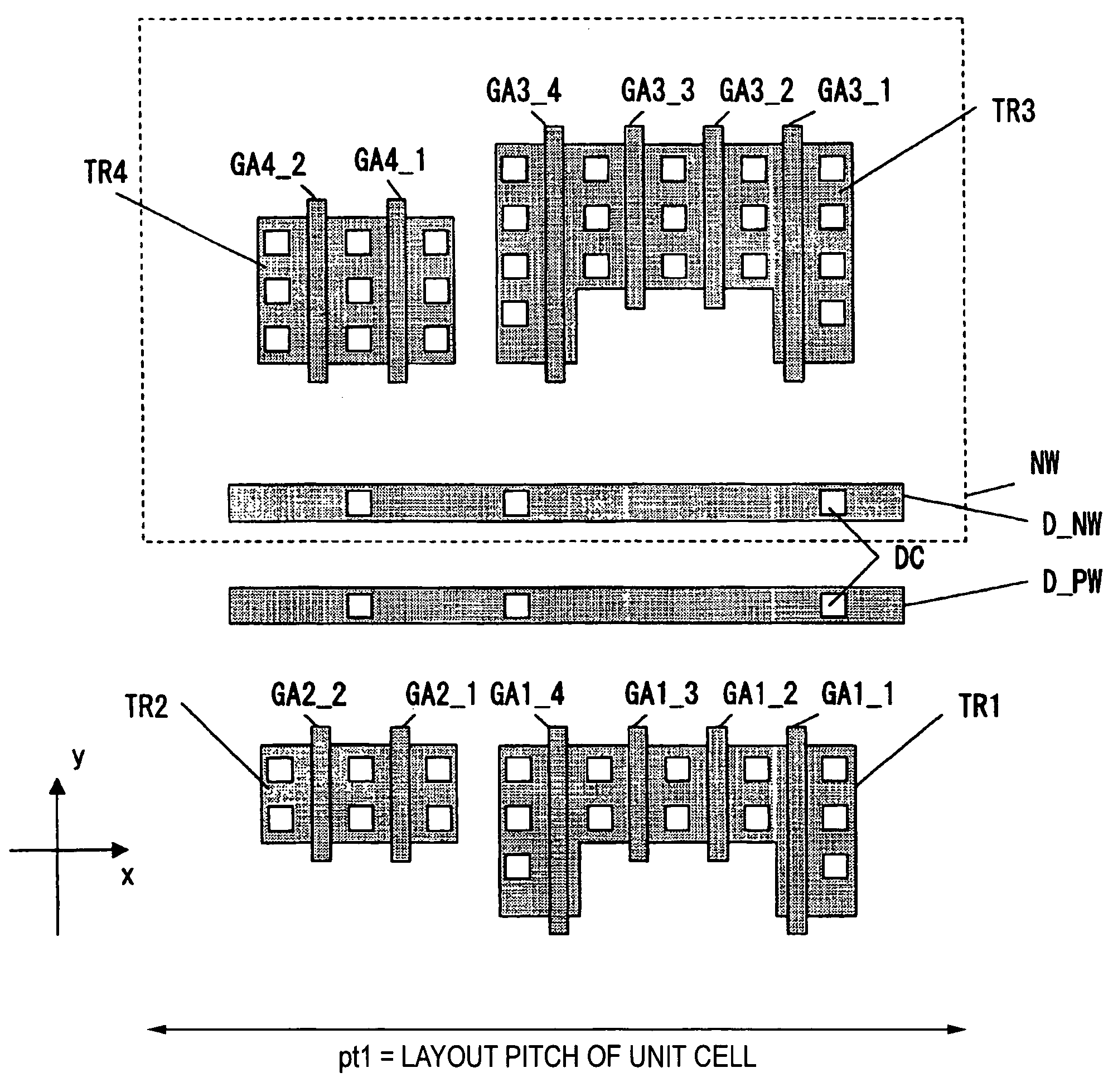
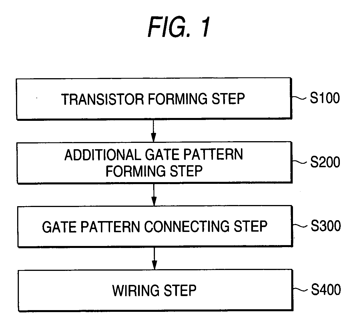
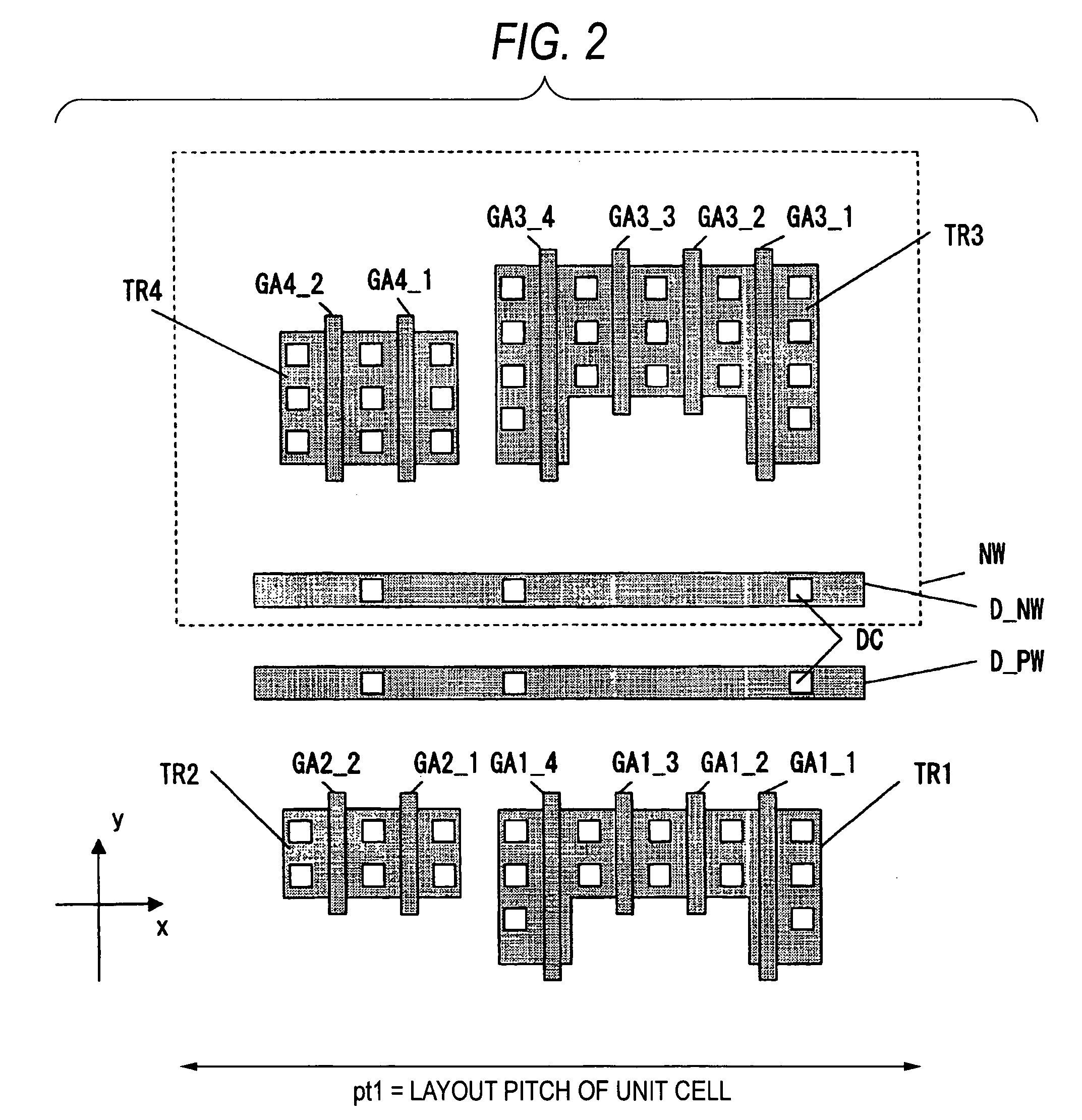
[0130]FIG. 1 is a diagram showing a flow of the layout design method of the invention. After a transistor forming step S100, an additional gate pattern forming step S200 of forming an additional gate pattern serving as a dummy gate in parallel with and at a fixed distance from a gate electrode of a transistor is performed, and a gate pattern connecting step S300 of connecting a gate pattern or a gate contact region to the formed gate electrode of the transistor and arranging the gate pattern or the gate contact region and a wiring step S400 of wiring a metal layer are executed. The respective steps will be hereinafter explained with layout design of a region surrounded by 33(A) of a latch circuit shown in FIG. 33 as an example.

[0131]FIG. 2 is a layout diagram of transistors TR1 to TR4 formed in the transistor forming step S100. The transistors TR1 and TR3 have gate electrodes GA1_1 to GA1_4 and GA3_1 to GA3_4 with different gate width. The transistors TR2 and TR4 ...

second embodiment

(Second Embodiment)

[0145]FIG. 12 is a diagram showing a flow of a layout design method according to a second embodiment of the invention. The layout design method in the second embodiment is different from the layout design method described in the first embodiment in that a transistor moving step S250 of moving a transistor is added after the additional gate pattern forming step S200, an additional gate pattern correcting step S500 of correcting a shape or adding an additional gate pattern anew such that the additional gate pattern arranged as the dummy gate meets the design rule is added after the wiring step S400, and a gate pattern connecting step S300′ is a partially corrected version of the gate pattern connecting step S300 in the first embodiment. The layout design method in this embodiment will be hereinafter explained centering on the steps changed from the first embodiment with layout design of a buffer section 13(A) of a decoder circuit shown in FIG. 13 as an example.

[014...

third embodiment

(Third Embodiment)

[0164]FIG. 27 is a diagram showing a flow of a layout design method according to a third embodiment of the invention. The layout design method in the third embodiment is different from the layout design method described in the second embodiment in that an additional gate pattern forming step S200′ is a partially corrected version of the additional gate pattern forming step S200′ in the second embodiment. The layout design method in this embodiment will be hereinafter explained concerning only changed steps.

[0165]FIG. 28 is a layout diagram in which a transistor TR8 is formed in the transistor forming step S100. Gate electrodes GA8_1 to 3 are arranged on the transistor TR8 and the gate electrodes GA8_2 and GA8_3 are arranged linearly and share a source region S8_1.

[0166]FIG. 30 is a diagram showing a flow of the additional gate pattern forming step S200′. The additional gate pattern forming step S200′ consists of an external additional gate pattern forming step S2...


PUM


Abstract

A layout design method for a semiconductor device includes a step of arranging transistors, a dummy gate forming step of forming dummy gates, which has a shape identical with a shape including gate electrodes or the gate electrodes and projected parts from active regions of the gate electrodes, in positions in parallel with and a fixed distance apart from the gate electrodes arranged at both ends in a gate length direction on active regions of the transistors and, when the transistors have plural gate electrodes with different gate widths, extending the projected parts to the outside of the active regions by a necessary length, a gate connecting step of, when gate patterns and contact regions are connected to the gate electrodes of the transistors, connecting the gate electrodes and the dummy gates according to a positional relation between the gate electrodes and the dummy gates, and a wiring step of wiring a metal layer. It is possible to design a semiconductor device having a smaller area than that in the past and with a less design man-hour.

Description

BACKGROUND OF THE INVENTION [0001] 1. Field of the Invention [0002] The present invention relates to a semiconductor device and a layout design method for the semiconductor device, and in particular to a semiconductor device and a layout design method for the semiconductor device that arrange dummy gates in order to control fluctuation in shapes of gate electrodes of transistors. [0003] 2. Description of the Related Art [0004] There is known a layout design method of arranging dummy gates in positions a fixed distance apart from gate electrodes of transistors such that gate patterns are arranged at equal intervals in order to control fluctuation in shapes of the gate electrodes of the transistors. JP-A-2000-200882 (FIG. 1) and JP-A-2000-223663 (FIG. 1) described below mention that the dummy gate is formed in a process identical with that for a gate electrode of an adjacent transistor, has an composition and a shape identical with the gate electrode, and is floating in terms of a pot...

Claims


Application Information

Patent Timeline
Patent Type & Authority Applications(United States)
IPC IPC(8): G06F17/50H01L21/82H01L21/822H01L21/8234H01L27/02H01L27/04H01L27/088H01L27/10
CPCG06F30/392H01L27/0207
Inventor HAYASHI, KOHTAROSHIBAYAMA, AKINORI
Owner SOCIONEXT INC
Why Eureka
Try Eureka