Display panel packaging method and packaging structure

a technology of display panel and packaging method, applied in the field of display technology, can solve the problem that the ultraviolet light cannot be reduced after finishing the packaging

Active Publication Date: 2021-12-30
SHENZHEN CHINA STAR OPTOELECTRONICS SEMICON DISPLAY TECH CO LTD
View PDF0 Cites 1 Cited by
  • Summary
  • Abstract
  • Description
  • Claims
  • Application Information

AI Technical Summary

Benefits of technology

[0005]The packaging structure in the prior art has problems that a packaging design of a single sealant structure cannot effectively block external moisture, and that an effect of a negative drifted electrical property of internal substrates due to ultraviolet light cannot be reduced after finishing packaging.

Problems solved by technology

The packaging structure in the prior art has problems that a packaging design of a single sealant structure cannot effectively block external moisture, and that an effect of a negative drifted electrical property of internal substrates due to ultraviolet light cannot be reduced after finishing packaging.

Method used


Image

  • Display panel packaging method and packaging structure
  • Display panel packaging method and packaging structure

Examples


Embodiment Construction

[0047]Embodiments are described below with reference to the appended drawings, and the drawings illustrate particular embodiments in which the present invention can be practiced.

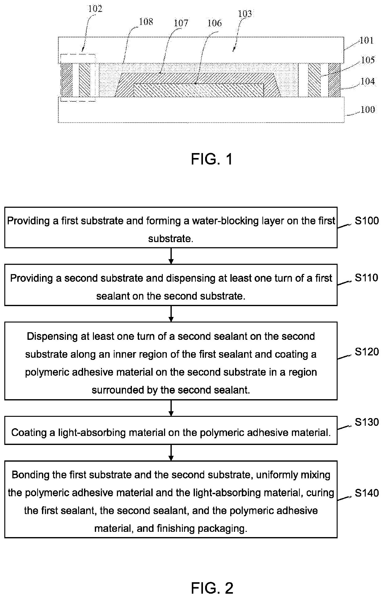
[0048]After components of a display panel are assembled, the display panel needs to be effectively packaged to prevent external moisture from entering the OLED display panel. Also, a package layer can protect the components to ensure lifetime of the display panel. The present invention provides a packaging structure, as shown in FIG. 1, which is a diagram of the packaging structure of a display panel of an embodiment of the present invention. A display panel includes a first substrate 100 and a second substrate 101 disposed opposite to the first substrate 100. The first substrate 100 can be a thin-film transistor (TFT) array substrate. In this embodiment, the first substrate 100 is described by using the TFT array substrate as an example.

[0049]An organic light-emitting diode (OLED) device layer 106 and a wat...


PUM

PropertyMeasurementUnit
polymericaaaaaaaaaa
transparentaaaaaaaaaa
self-luminosityaaaaaaaaaa

Abstract

The present invention provides a display panel packaging method and a packaging structure. The display panel packaging method includes: providing a first substrate and forming a water-blocking layer, dispensing a sealant on a second substrate, coating a polymeric adhesive material in a region surrounded by the sealant, coating a light-absorbing material on the polymeric adhesive material, bonding the two substrates and uniformly mixing the polymeric adhesive material and the light-absorbing material to form a uniformly mixed film, and curing them and finishing packaging. This display panel packaging is effective.

Description

FIELD OF INVENTION[0001]The present invention is related to the field of display technology, and specifically to a display panel packaging method and a packaging structure.BACKGROUND OF INVENTION[0002]Compared to liquid crystal display devices, organic light-emitting diode (OLED) display devices have advantages of self-luminosity, fast response times, and light weight, and have become an emerging technology in the display field.[0003]After components of an OLED display panel are assembled, the OLED display panel needs to be effectively packaged to prevent external moisture from entering the OLED display panel. Currently, main processes for packaging the OLED display panel are: dispensing a sealant on a hard packaging cover plate, disposing a getter on an inner side of the sealant, assembling the packaging cover plate with the sealant and a thin-film transistor (TFT) substrate, curing the sealant, and finishing packaging. Because the sealant is generally made of simple organic materi...

Claims


Application Information

Patent Timeline
Patent Type & Authority Applications(United States)
IPC IPC(8): H01L51/52H01L51/56
CPCH01L51/5246H01L51/56H01L51/5284H01L51/5259H10K50/84H10K50/844H10K71/00H10K71/50H10K50/8426H10K50/865H10K50/846
Inventor MIAO, YANGLI, JINCHUAN
Owner SHENZHEN CHINA STAR OPTOELECTRONICS SEMICON DISPLAY TECH CO LTD
Why Eureka
Try Eureka