Light microscope and microscopy method
Pending Publication Date: 2022-01-20
CARL ZEISS MICROSCOPY GMBH
0 Cites 0 Cited by
AI-Extracted Technical Summary
Problems solved by technology
The excitation becomes inefficient so that higher illuminating light intensities become necessary, which in turn can lead to photodamage of the sample.
The part of the sample light that hits the Shack-Hartmann sensor is not available for the generation of the sample image.
A significant part of the sample light is thus unusable for the actual imaging process in conventional light microscopes.
A further disadvantage of conventional light microscopes is their low compensation speed.
An individual compensation via the adaptive o...
Method used
[0072]It is possible to improve the quality of a captured microscope image by means of a subsequent computation that uses the knowledge of the wavefront 16. Conventional microscopes use separate light detectors for the direct wavefront measurement and the capture of a microscope image. This is due to the fact that the sample image is captured by means of a very fast scan of the sample, which requires very fast detectors. The sensors used for wavefront measurement, however, are generally substantially slower. It is consequently not possible to allocate the signals measured by a wavefront sensor to a single sample point so that they are not used for the measurement of the sample image. A large part of the sample light intensity is thus lost in conventional microscopes as a result of the wavefront measurement and is not available for the capture of the sample image.
[0078]In addition to the arrangement of the microlens array in the pupil plane, a setting of the illumination intensity or of an illumination pulse frequency is also relevant in order to ideally avoid a saturation of the light detector. The electronics unit can be configured to evaluate whether a saturation is probable based on the measurement signals of the detector elements captured up to that point during a scan. A saturation can be presumed, for example, when a photon count of one or more detector elements exceeds a predetermined threshold value. The electronics unit can then immediately reduce an illumination intensity and/or pulse frequency of the light source.
[0090]In step S4, a focus position is computed for each microlens from the measurement signals. A wavefront, i.e., for example, the wavefront at the objective pupil, is computed on this basis. For a better signal-to-noise ratio, the measurement signals relating to the same microlens that have been captured for successive sample points can also be combined or added together and used conjointly for the determination of the wavefront. In this case, an individual wavefront is not determined for each sample point. Rather, a wavefront is respectively computed for given areas. This is suitable when the regions essentially correspond to a so-called isoplanatic patch.
[0093]After the entire sample has been scanned, step S6 follows. A sample image is computed in this step from the sample point signals while taking into account the determined wavefronts. This can be achieved, for example, by combining the sample point signals into a raw image. Each sample point signal corresponds to an image point of the raw image. A deconvolution of the raw image is then carried out, for which the determined wavefronts are used. The deconvolution occurs separately for different raw image areas, a wavefront having been respectively determined for each raw image area. The raw image areas can be set according to isoplanatic patches. To this end, it is possible to identify a change in successive focus positions determined for the same microlens, i.e. a difference in the focus position of a microlens for different, successively illuminated sample points. There are only slight changes in the scanned medium within the isoplanatic patch so that the changes in the focus positions behind the respective microlenses are consequently also slight. If the change remains below a predefined threshold value, an isoplanatic path can be assumed. The focus positions of the same microlens for these successively illuminated sample points are added together accordingly and used conjointly for the determination of a wavefront region. It is also possible to use a plurality of focus positions for the comparison with the threshold value and the assessment of how far an isoplanatic patch extends. It can, however, also be expedient to average areas exhibiting a strong variation. It is possible, for example, to take into account only...
Benefits of technology
[0014]The indication of a light microscope and a microscopy method which allow a sample imaging and a wavefront measurement that ...
Abstract
A light microscope having a scanner for scanning a sample with illuminating light and a light detector for measuring sample light. A microlens array having a plurality of microlenses is arranged in front of the light detector in the region of a pupil plane. The light detector respectively has a plurality of detector elements behind each microlens and has a complete readout frequency of at least 100 kHz. By means of the detector elements arranged behind the respective microlens, a wavefront datum regarding the sample light is determined. Moreover, a sample point signal is computed from signals of the detector elements. Illuminating light is successively deflected onto different sample points with the scanner and corresponding sample point signals are captured, wherein, for at least some of the different sample points, a corresponding wavefront datum is also determined. The determined wavefront data can be taken into account in a calculation of a sample image from the plurality of sample point signals.
Application Domain
MicroscopesFluorescence/phosphorescence
Technology Topic
Sample imageWavefront +6
Image
Examples
- Experimental program(1)
Example
DETAILED DESCRIPTION OF THE DRAWINGS
[0063]In general, similar components and components that function in a similar manner are designated in the figures by the same references.
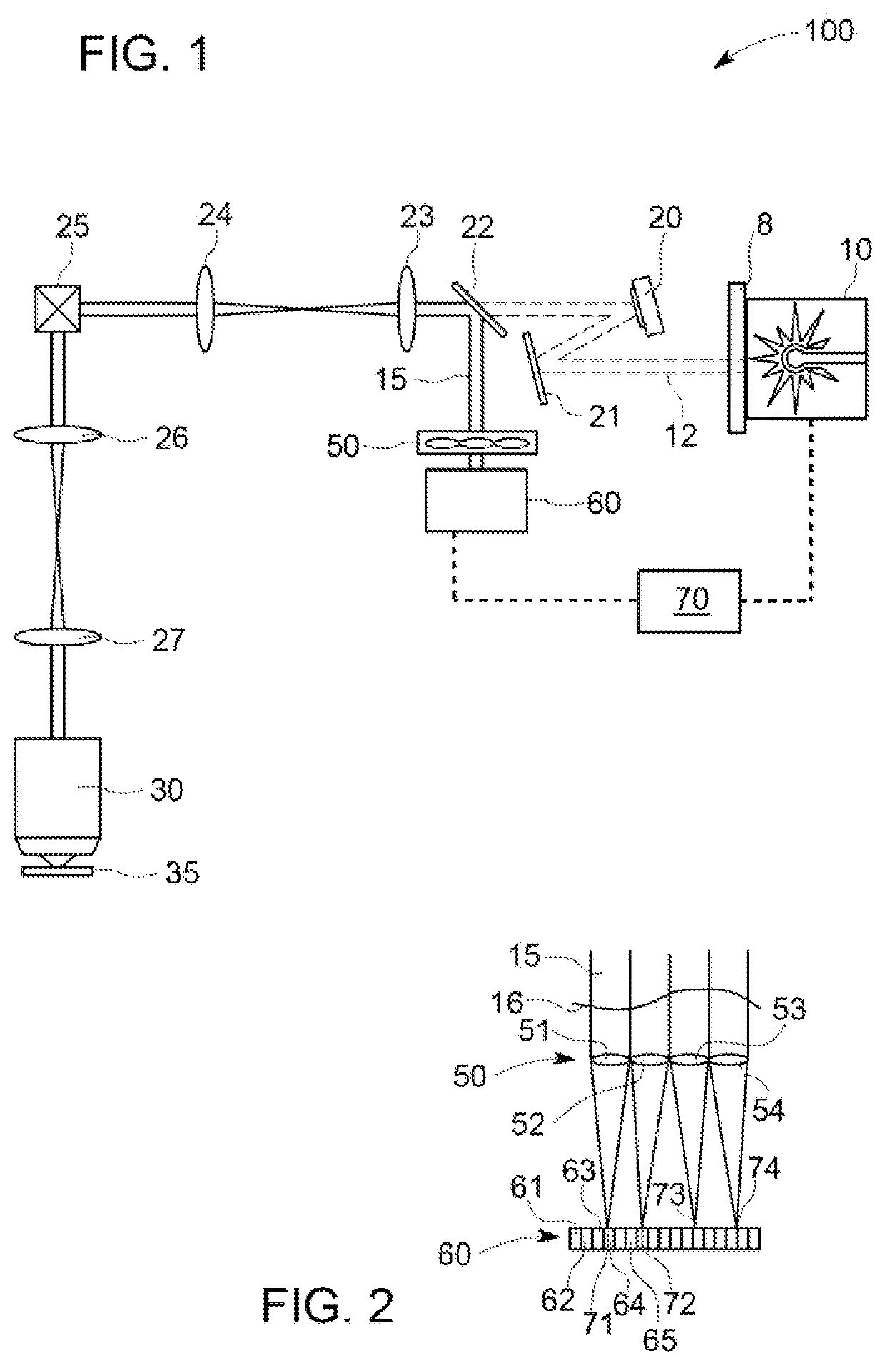
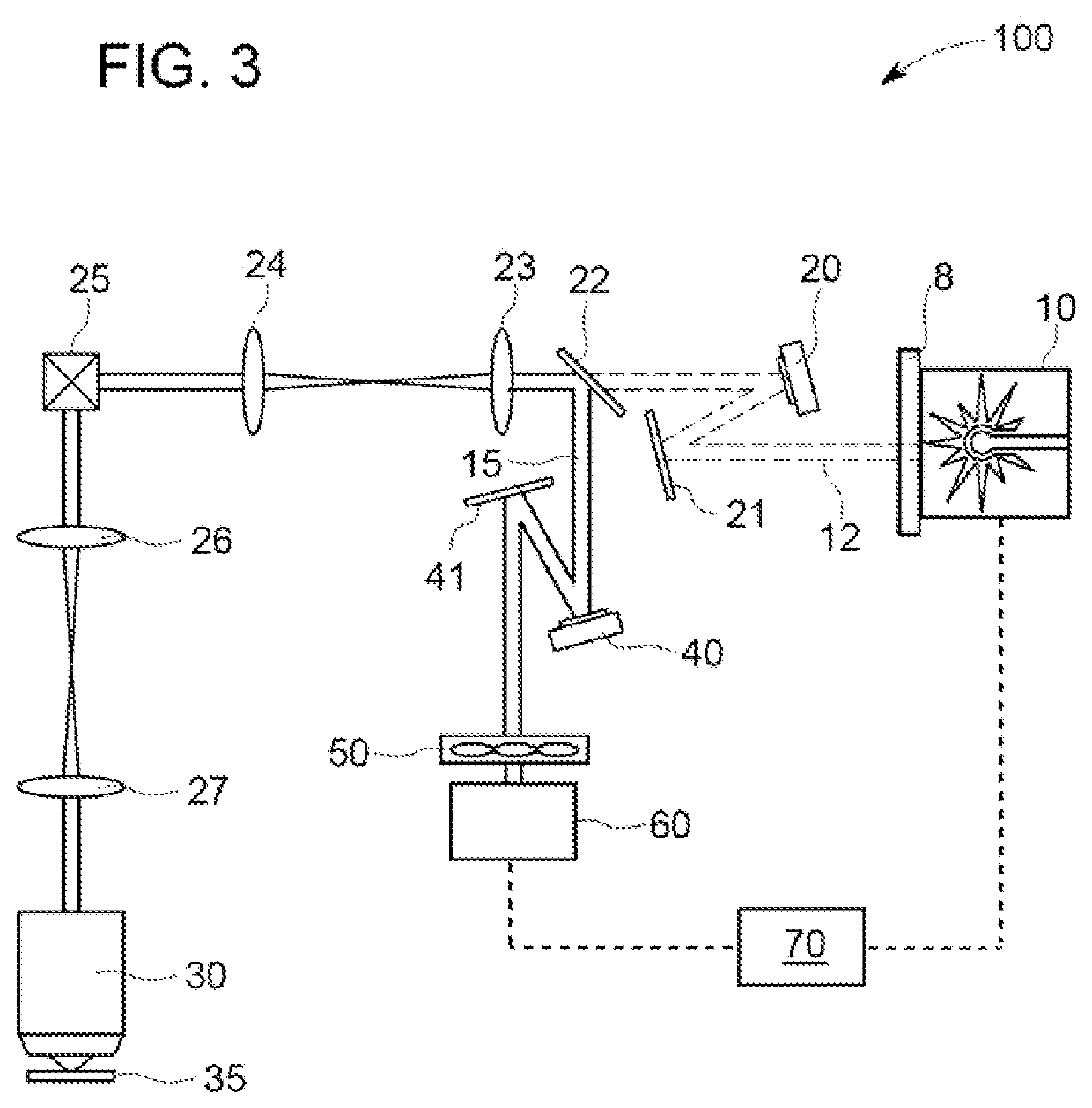
[0064]FIG. 1 shows an example embodiment of a light microscope 100 according to the invention designed as a laser scanning microscope.
[0065]The light microscope 100 comprises a light-source port 8 via which illuminating light 12 of a light source 10 can be coupled. The light source 10 illustratively comprises one or more lasers. Via optional optic elements (for example, a mirror arrangement not illustrated here), illuminating light from one or a plurality of lasers can be merged into the same light path.
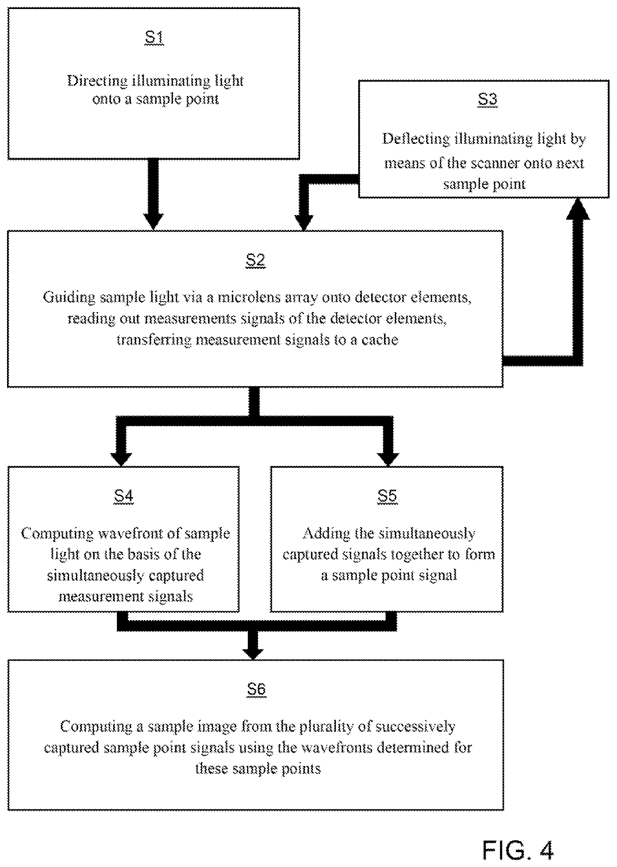
[0066]A sample 35 is scanned with the illuminating light 12. This means that the illuminating light 12 is focussed on a sample point and different sample points are successively illuminated according to a scanning movement. A plurality of optic elements 21, 23, 24, 26, 27 and an objective 30 are provided for conducting the illuminating light 12 to the sample 35. A scanner 25 is used to scan the sample 35 with the illuminating light 12. The scanner 25 can comprise, for example, two movable scanning mirrors or some other number of scanning mirrors. In principle, any orientable beam deflection device is conceivable as the scanner, for example an acousto-optic beam deflector.
[0067]Sample light 15—which can be, for example, fluorescent light or phosphorescent light—is emitted by the sample 35. The illuminating light can in particular be radiated in pulses and be used for a multiphoton-fluorescence excitation. Sample light 15 is consequently only emitted from a particularly small sample area and has a shorter wavelength than the illuminating light 12.
[0068]In the illustrated descanned structure, the sample light 15 is returned via the objective 30, the scanner 25 and the optic elements 27, 26, 24, 23. It is spatially separated from the illuminating light 12 by means of a beam splitter 22. The beam splitter 22 can be designed, for example, to either reflect or transmit light depending on its wavelength. The sample light 15 is then guided via a microlens array 50 onto a light detector 60.
[0069]An enlargement of the microlens array 50 and the subsequent light detector 60 is illustrated in FIG. 2. The microlens array 50 comprises a plurality of microlenses 51-54 arranged next to one another in a two-dimensional pattern. The light detector 60 comprises a plurality of detector elements per microlens 51-54. In FIG. 2, a plurality of detector elements 61-65 are located behind the first microlens 51, while the detector elements behind the other microlenses 52-54 are not provided with reference numbers for the sake of clarity. A diameter of a microlens 51 is accordingly larger than a distance between adjacent detector elements 61, 62, for example at least 5 times larger.
[0070]The microlens array is arranged here in a pupil plane or in the area of a pupil plane. The advantage of this arrangement is explained in greater detail below. The distance of the detector elements 61-65 from the microlenses 51-54 is equal or essentially equal to the focal length of the microlenses 51-54. Focus positions 71-74 of sample light 15 on the detector elements thus depend on the shape of the wavefront 16 when it strikes the microlenses 51-54. A section of the wavefront 16 of the total sample-light cross-section can be analysed via each microlens 51-54 by means of a determination of the focus positions (i.e. a determination of the focus of the received light intensity/number of photons) with the respective detector elements 61-65 behind each microlens 51-54. The wavefront 16 can be computed from this plurality of focus positions 71-74. In more general terms, a wavefront datum that describes or characterizes the wavefront 16 can be determined from the respective intensity distributions behind the microlenses.
[0071]The wavefront 16 is influenced by media that the sample light 15 traverses. In particular optically complex samples or sample media thus have a relevant impact on the wavefront 16. In the case of biological samples, different cell components can have very different effects, in particular when deeper cell layers are analysed. Non-biological samples, for example electronic components, can also have complex structures that significantly influence the wavefront.
[0072]It is possible to improve the quality of a captured microscope image by means of a subsequent computation that uses the knowledge of the wavefront 16. Conventional microscopes use separate light detectors for the direct wavefront measurement and the capture of a microscope image. This is due to the fact that the sample image is captured by means of a very fast scan of the sample, which requires very fast detectors. The sensors used for wavefront measurement, however, are generally substantially slower. It is consequently not possible to allocate the signals measured by a wavefront sensor to a single sample point so that they are not used for the measurement of the sample image. A large part of the sample light intensity is thus lost in conventional microscopes as a result of the wavefront measurement and is not available for the capture of the sample image.
[0073]These drawbacks are overcome with the invention. The light microscope 100 uses the same light detector 60 and the same measurement data/signals captured by the same to determine both the wavefront as well as the sample point signals, from which an adjusted sample image that takes the determined wavefront into account is computed. Sample light that would otherwise not be available for the acquisition of the sample image is not diverted for a wavefront measurement.
[0074]In particular the aspects described in the following are relevant in this connection.
[0075]The light detector 60 has a complete readout rate of at least 100 kHz, which denotes the frequency at which all detector elements of the detector 60 are read out. The readout rate can thus be at least as high as the scan rate, i.e. the inverse readout frequency can be lower than or equal to the inverse pixel dwell time. In principle, it is sufficient when a part and not all of the detector elements of the light detector 60 are read out for a scanned sample point. The descriptions relating to detector elements 61-65 of the detector 60 can thus also be understood as referring to a part and not all of the detector elements. It is thus sufficient when the time for reading out the detector elements 61-65 used for the computation of the image is equal to or less than a pixel dwell time, while a time for reading out all detector elements could also be greater than the pixel dwell time.
[0076]Photon-counting detector elements can be preferable as detector elements 61-65, in particular single-photon avalanche diodes (SPAD). Photon-counting detector elements have a very high time resolution, which is substantially better than the time resolution of, for example, EMCCD sensors, which are often used for wavefront measurements. The photon-counting detector elements are operated so that their readout time (i.e. the duration of a photon count) corresponds to the pixel dwell time during which a sample point (pixel) is illuminated via the scanner. A photon count is carried out for each sample point.
[0077]In order for a photon-counting detector element to provide a precise result, it should reach saturation as rarely as possible. Following the reception of a photon and the triggering of a current avalanche, a dead time elapses before the next photon can be detected. In order for a saturation of the light detector to occur as rarely as possible, it is expedient when the light detector comprises a large number of detector elements, for example over 10,000, which are arranged behind a microlens array in the pupil plane. The sample light emitted by a sample point illuminates the pupil approximately evenly, i.e. substantially more evenly than an image plane. The parts of the sample light are thus distributed substantially more evenly onto the plurality of microlenses with their subsequent detector elements in the pupil plane.
[0078]In addition to the arrangement of the microlens array in the pupil plane, a setting of the illumination intensity or of an illumination pulse frequency is also relevant in order to ideally avoid a saturation of the light detector. The electronics unit can be configured to evaluate whether a saturation is probable based on the measurement signals of the detector elements captured up to that point during a scan. A saturation can be presumed, for example, when a photon count of one or more detector elements exceeds a predetermined threshold value. The electronics unit can then immediately reduce an illumination intensity and/or pulse frequency of the light source.
[0079]An electronics unit 70 controls the light detector 60, in particular the processes described for image capture such as the computation of wavefront data, the aggregation of measurement signals of the light detector to form a sample point signal/confocal signal, as well as the computation of a sample image from the plurality of successively captured sample point signals while taking into account the wavefront data. The electronics unit 70 can control further microscope components, in particular the light source 10, the adaptive optic element 20 and/or the scanner 25.
[0080]In the example embodiment shown in FIG. 1, the adaptive optic element 20 is located in the illuminating light path. In a variant of this embodiment, the adaptive optic element 20 can be arranged in a common light path of the illuminating light 12 and sample light 15, in particular between the beam splitter 22 and the objective 30. Sample light 15 in this case can also be conducted via the adaptive optic element 20, which can manipulate its wavefront.
[0081]In a variant of the example embodiment of FIG. 1, a pinhole aperture is added, for example in a conjugate plane of the sample plane in which the sample 35 is arranged. This plane can lie between the objective 30 and the beam splitter 22, in particular in the illustrated intermediate image plane between the optic elements 26 and 27 or in the intermediate image plane between the optic elements 23 and 24. In this case, the adaptive optic element 20 or a further adaptive optic element can be arranged between the sample 35 and the pinhole aperture.
[0082]A modified example embodiment is shown in FIG. 3. This embodiment differs from the one shown in FIG. 1 in that an adaptive detection optic 40 is added in the detection light path. The adaptive detection optic 40 can be formed like the adaptive optic element 20 described above. In the example illustrated in FIG. 3, sample light 15 first strikes the adaptive detection optic 40 and subsequently the microlens array 50, although this order can also be reversed. An optic element 41, here a mirror, for relaying the sample light 15 is depicted illustratively in FIG. 3. The adaptive detection optic 40 can be provided in addition to the adaptive optic element 20, as depicted, although alternatively the adaptive optic element 20 can also be omitted. The adaptive detection optic 40 can essentially be controlled by the electronics unit 70 as described for the adaptive optic element 20. In particular, the adaptive detection optic 40 can be adjusted during a sample scan as a function of the currently measured wavefront data.
[0083]The individual method steps for image capture and wavefront measurement are illustrated in FIG. 4. The electronics unit of an example embodiment of the light microscope according to the invention is configured to carry out these method steps in an automated manner, in particular by means of a corresponding control of the light source, the scanner and the light detector.
[0084]In method step S1, illuminating light is focussed on a sample point. The illuminating light can be, for example, a light pulse for multiphoton excitation.
[0085]According to step S2, sample light emanating from the sample point is conducted via the microlens array onto the detector elements. Following the pixel dwell time, which is determined by the speed of the scanner and the intended resolution, the measurement signals of the detector elements are read out. In the case of photon-counting detector elements, each measurement signal represents a measured number of photons. These measurement signals are temporarily stored in a data memory.
[0086]In step S3, the illumination light is deflected by means of the scanner onto a next sample point. The scanning movement can be carried out continuously whereby the steps S2 and S3 occur simultaneously. A division of the sample into sample areas can be assumed in this case, wherein a sample point is considered the same when the scanner moves the illuminating light within the same sample area; if the illuminating light hits a subsequent, adjacent sample area, this is designated a deflection to the next sample point.
[0087]Sample light is likewise measured for the next sample point and the corresponding measurement signals stored in the data memory/cache in accordance with step S2.
[0088]The entire sample or the entire region of interest (ROI) of the sample is scanned in this manner.
[0089]The steps S4 and S5 are carried out during the scanning of the sample or after the sample has been entirely scanned.
[0090]In step S4, a focus position is computed for each microlens from the measurement signals. A wavefront, i.e., for example, the wavefront at the objective pupil, is computed on this basis. For a better signal-to-noise ratio, the measurement signals relating to the same microlens that have been captured for successive sample points can also be combined or added together and used conjointly for the determination of the wavefront. In this case, an individual wavefront is not determined for each sample point. Rather, a wavefront is respectively computed for given areas. This is suitable when the regions essentially correspond to a so-called isoplanatic patch.
[0091]It can be expedient for the determination of the wavefronts to be carried out very quickly during scanning. To this end, the determination of the focus positions can be carried out in parallel, for example in a graphics processing unit (GPU). This method is particularly well suited to the determination of the focus positions as the allocation of the sensor elements to the microlenses and thus to the lateral areas of the wavefront is fixed in advance. A processor within the GPU can thus be allocated to each microlens so that the algorithm for determining the focus position can be applied simultaneously for each microlens within the array.
[0092]In step S5, the measurement signals captured with the plurality of detector elements for a sample point are combined. In particular the measurement signals of all detector elements, i.e. all simultaneously captured signals, can be added together/integrated. This yields a sample point signal. A sample point signal is thus captured per scanned sample point. The sample point signal can consequently be based on the entirety of the sample light detected simultaneously. No part of the sample light, which would otherwise be lost for the sample point signal, is diverted for wavefront measurement. Rather, the wavefront(s) and the sample point signals are determined from the same measurement signals. In particular, all measurement signals can be used both for the wavefront determination and for the determination of the sample point signals.
[0093]After the entire sample has been scanned, step S6 follows. A sample image is computed in this step from the sample point signals while taking into account the determined wavefronts. This can be achieved, for example, by combining the sample point signals into a raw image. Each sample point signal corresponds to an image point of the raw image. A deconvolution of the raw image is then carried out, for which the determined wavefronts are used. The deconvolution occurs separately for different raw image areas, a wavefront having been respectively determined for each raw image area. The raw image areas can be set according to isoplanatic patches. To this end, it is possible to identify a change in successive focus positions determined for the same microlens, i.e. a difference in the focus position of a microlens for different, successively illuminated sample points. There are only slight changes in the scanned medium within the isoplanatic patch so that the changes in the focus positions behind the respective microlenses are consequently also slight. If the change remains below a predefined threshold value, an isoplanatic path can be assumed. The focus positions of the same microlens for these successively illuminated sample points are added together accordingly and used conjointly for the determination of a wavefront region. It is also possible to use a plurality of focus positions for the comparison with the threshold value and the assessment of how far an isoplanatic patch extends. It can, however, also be expedient to average areas exhibiting a strong variation. It is possible, for example, to take into account only certain aberration orders this way. The flexibility of the spatial averaging of the aberrations via certain focus positions is an essential difference vis-à-vis conventional methods in which the number of sample points over which measurement signals for the computation of the wavefront are averaged is determined in advance. This number can be set in a variable manner with the invention. In particular, the measurement signals relating to different quantities of sample points are used to compute a wavefront for a single sample image in an area-dependent manner. In this manner, a sample image is output in step S6, the image quality of which is improved compared to conventional methods. Step S6 can optionally provide a user with different options as to how the wavefront data is to be determined and a sample image computed from the signals. The options can differ in particular with respect to how successively captured wavefront data/focus positions are averaged, in particular in terms of the number of signals for successively scanned sample points to be averaged. This makes it possible to define isoplanatic areas of different sizes for the computation of a single sample image.
[0094]By taking the determined wavefront into account in the adjusted computation of the sample point signals as described, undesired aberrations of the sample light can be effectively compensated. An adaptive optic does not have to be provided for this purpose. This makes it possible to realize a fast imaging at a lower cost since a slower correction via a feedback loop and an adaptive optic is no longer necessary. An alternative method variant in which a feedback loop with an adaptive optic is used is illustrated in FIG. 5. This illustration differs from the preceding figure in that the wavefront determined in step S4 is already used during the scan. Step S7, in which the wavefront determined for one or more sample points is used to set an adaptive optic element in the illuminating light path, thus follows step S4. Illuminating light is emitted onto the next sample point with this setting the next time step S2 is carried out. Alternatively or in addition to the setting of an adaptive optic element in the illuminating light path, it is also possible to set an adaptive detection optic in step S7, in which case the steps S7 and S3 can also occur simultaneously.
[0095]Adjusting the adaptive optic element can take longer than an adjustment of the scanner, i.e. the cycle of the steps S2 and S3 shown in FIG. 5 can occur more often than the step S7.
[0096]Alternatively, it is also possible to carry out a plurality of settings of the adaptive optic element for a sample point to be scanned in rapid succession. This way, it is possible to try out different settings of the adaptive optic element for the same scanning position in order to test different aberrations. FIG. 5 illustrates a variant of this embodiment in that the scanner adjustment of step S3 does not always follow the adjustment of the adaptive optic element in step S7, but rather it is also possible to go directly to step S2. Step S4 only occurs optionally between the steps S2 and S7, as the data evaluation of the steps S4 and S5 can generally only be carried out upon completion of a sample scan.
[0097]The adaptive optic element 20 can be, for example, a spatial light modulator (SLM) or a deformable mirror. As step S4 is carried out before the scan for the sample image determination is completed, the data regarding the wavefront can be used to set the adaptive optic element 20 in step S7. The adaptive optic element 20 is set so that a generated wavefront deformation is at least partially compensated. The aforementioned features can apply, additionally or alternatively, to the adaptive detection optic 40. For good results, the illuminating light should still be directed at the same isoplanatic patch for which the wavefront was determined in step S4. This advantage can also be exploited in multipoint scanning with a plurality of illuminating points, as described in greater detail in the following.
[0098]The captured data regarding the wavefront can also be stored for the realization of subsequent images of the same sample. The data regarding the wavefront can thereby be subsequently evaluated in different ways in order to compute a sample image ideally unaffected by undesired aberrations.
[0099]In a variant of the embodiment of FIG. 1, a plurality of illuminating points scan the sample simultaneously and at a distance from one another. The illuminating points can be produced by a plurality of units of the light source 10, for example a plurality of lasers, or by a spatial splitting of the illuminating light 12. A plurality of sample light beams caused by different illuminating points are to be detected separately. To this end, a sample-light beam splitter can be arranged in front of the microlens array 50, in particular between the beam splitter 22 and the microlens array 50. The sample-light beam splitter can be arranged in an intermediate image plane and be, for example, an array of lenses or an array of mirrors. Sample light beams caused by different illuminating points are thereby guided into different detection light paths, in which a microlens array with a subsequent light detector is respectively arranged. The detection light paths can lead to different areas of the same microlens array so that different sample light beams hit different detector elements. This way, a plurality of sample areas can be scanned simultaneously.
[0100]The illuminating beams can either be guided over separate sample areas or successively scan the same sample areas. It can be expedient for an enhanced image quality to scan the same sample point repeatedly. In this case, as described above, the wavefront data that was determined for a sample point can also be used for the setting of the illumination intensity and/or of the adaptive optic element during the repeated scanning of the same sample point. For example, if the illumination intensity was too high for this sample point during the first scan, the illumination intensity is (temporarily) reduced. Moreover, the adaptive optic element can be set so that a wavefront deformation from this sample point is at least partially compensated. A separate adaptive optic element can be used for each illuminating light beam, wherein the latter should be clearly propagated from a pupil plane so that the individual illuminating light beams can be addressed separately by the adaptive optic elements. The definition of the isoplanatic patches in advance then merely represents a precondition for the determination of the wavefront data, which is adapted to the sample or the sample region according to the described method.
[0101]Conventionally, the size and position of the sample areas for which the adaptive optic element is to adopt a given correction setting are defined in advance, i.e. before the start of the scan. The type of correction setting performed occurs as a function of data captured during the scan. The size and the position of the sample areas for which the correction setting is carried out with the adaptive optic element, however, are fixed. With the invention, on the other hand, it is possible to define the size and position of the sample areas for which the same setting is performed with the adaptive optic element in a variable manner during the scan.
[0102]It is thus possible with the light microscope of the present invention to improve the quality of a sample image using a wavefront measurement without losing any part of the sample light for the capture of the sample image as a result of the wavefront measurement.
[0103]While the invention has been illustrated and described in connection with currently preferred embodiments shown and described in detail, it is not intended to be limited to the details shown since various modifications and structural changes may be made without departing in any way from the spirit of the present invention. The embodiments were chosen and described in order to best explain the principles of the invention and practical application to thereby enable a person skilled in the art to best utilize the invention and various embodiments with various modifications as are suited to the particular use contemplated.
LIST OF REFERENCES
[0104]8 Light source port
[0105]10 Light source
[0106]12 Illuminating light
[0107]15 Sample light
[0108]16 Wavefront
[0109]20 Adaptive optic element
[0110]21, 23, 24, 26, 27 Optic elements
[0111]22 Beam splitter
[0112]25 Scanner
[0113]30 Objective
[0114]35 Sample
[0115]40 Adaptive detection optic
[0116]41 Optic element
[0117]50 Microlens array
[0118]51-54 Microlenses of the microlens array
[0119]60 Light detector
[0120]61-65 Detector elements of the light detector
[0121]70 Electronics unit
[0122]71-74 Focus positions behind the microlenses 51-54
[0123]100 Light microscope
[0124]S1-S7 Method steps
PUM


Description & Claims & Application Information
We can also present the details of the Description, Claims and Application information to help users get a comprehensive understanding of the technical details of the patent, such as background art, summary of invention, brief description of drawings, description of embodiments, and other original content. On the other hand, users can also determine the specific scope of protection of the technology through the list of claims; as well as understand the changes in the life cycle of the technology with the presentation of the patent timeline. Login to view more.