Method of manufacturing semiconductor device

a manufacturing method and semiconductor technology, applied in semiconductor devices, semiconductor/solid-state device details, electrical devices, etc., can solve the problem of reducing the yield of semiconductor devices, and achieve the effect of suppressing electrostatic breakdown

Active Publication Date: 2022-01-27
MITSUBISHI ELECTRIC CORP
View PDF0 Cites 1 Cited by
  • Summary
  • Abstract
  • Description
  • Claims
  • Application Information

AI Technical Summary

Benefits of technology

The present disclosure describes a method for manufacturing a semiconductor device by bonding a second electrode material with a shorting part, sealing the conductor plate and semiconductor elements with resin, and grinding the resin to remove the shorting part and expose the second electrode material. This method helps prevent electrostatic breakdown, especially in configurations involving semiconductor elements with a sense cell part.

Problems solved by technology

In International Publication No. 2020 / 110170, for example, in a case where a semiconductor element including a main cell part and a sense cell part (for example, a current sense cell) having a smaller flow dividing ratio than the main cell part is sealed with a sealing resin, if the sealing resin covering a surrounding area of the semiconductor element takes charge, there is a problem that an electrostatic breakdown occurs in the sense cell part at a time of handling the semiconductor device, particularly at a time of grinding an upper surface of the sealing resin to expose each conductor piece, and a yield of the semiconductor device decreases.

Method used


Image

  • Method of manufacturing semiconductor device
  • Method of manufacturing semiconductor device
  • Method of manufacturing semiconductor device

Examples


embodiment 1

[0052]

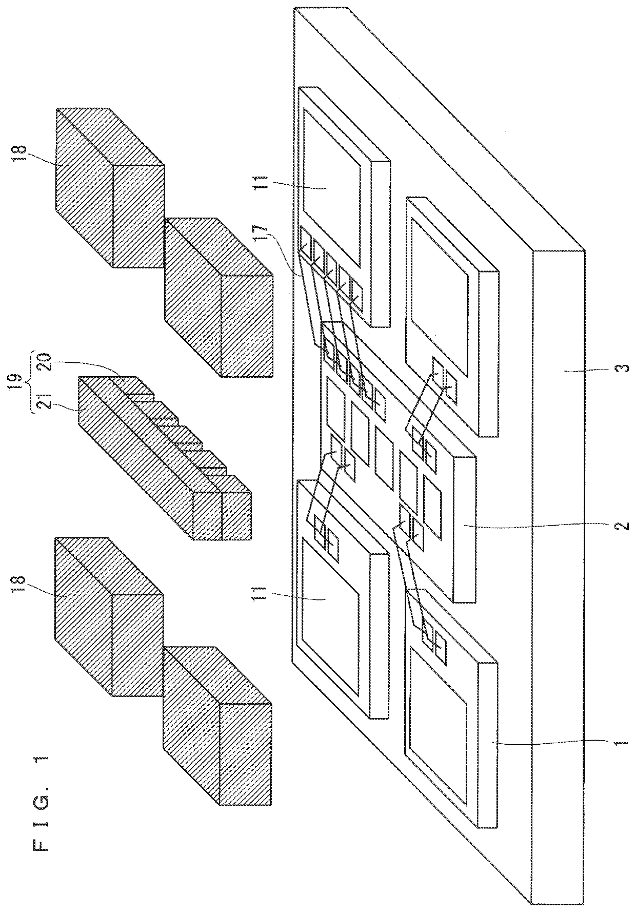
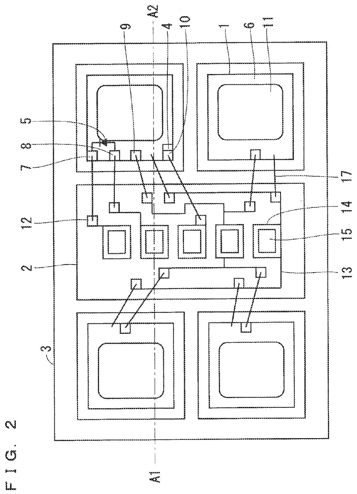
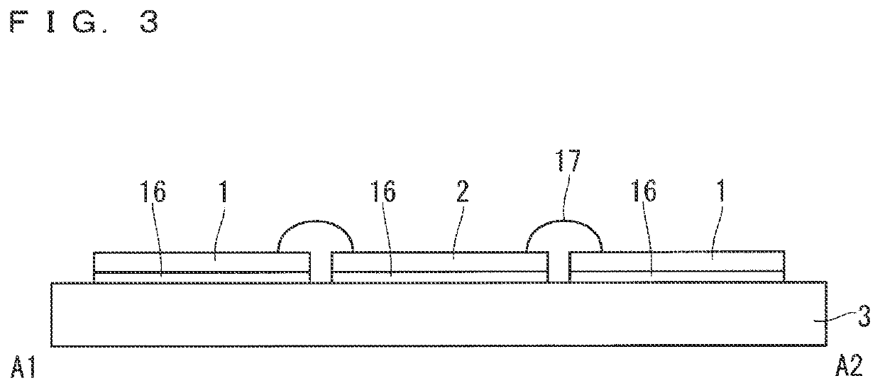
[0053]FIGS. 1 to 12 are diagrams for describing a method of manufacturing a semiconductor device according to an embodiment 1. FIG. 13 is a flow chart illustrating an example of the method of manufacturing the semiconductor device according to the embodiment 1. The method of manufacturing the semiconductor device according to the embodiment 1 is described hereinafter with reference to FIGS. 1 to 13.

[0054]As illustrated in FIGS. 1 to 3, in a first bonding process of Step S11 in FIG. 13, a relay substrate 2 and a plurality of semiconductor elements 1 are bonded on a conductor plate 3 using a bonding material 16.

[0055]The semiconductor element 1 is a composite compound semiconductor element made of SiC, for example, and is made up of a metal oxide semiconductor field effect transistor (MOSFET), for example. In the embodiment 1, the four semiconductor elements 1 are bonded on the conductor plate 3, and one of the four semiconductor elements 1 includes a main cell part and a sense ...

embodiment 2

[0081]

[0082]FIGS. 14 to 28 are diagrams for describing a method of manufacturing a semiconductor device according to an embodiment 2. The method of manufacturing the semiconductor device according to the embodiment 2 is described hereinafter with reference to FIGS. 14 to 28, however, the description is mainly focused on a process different from the method of manufacturing the semiconductor device according to the embodiment 1. Each process of manufacturing the semiconductor device according to the embodiment 2 is similar to that in the flow chart illustrated in FIG. 13.

[0083]As illustrated in FIGS. 17 to 19, in a third bonding process of Step S14 in FIG. 13, a second electrode material 24 is bonded to the connection film 15 provided on each second pad part 14 of the relay substrate 2 using the bonding material 22. The second electrode material 24 includes an insulating material 25 and the plurality of connection parts 20. The connection parts 20 are integrally formed by the insulati...

embodiment 3

[0093]

[0094]FIGS. 32 to 43 are diagrams for describing a method of manufacturing a semiconductor device according to an embodiment 3. FIG. 44 is a flow chart illustrating an example of the method of manufacturing the semiconductor device according to the embodiment 3. The method of manufacturing the semiconductor device according to the embodiment 3 is described hereinafter with reference to FIGS. 32 to 44, however, the description is mainly focused on a process different from the method of manufacturing the semiconductor device according to the embodiment 1.

[0095]The semiconductor device according to the embodiment 3 does not include the relay substrate 2. Accordingly, each process illustrated in FIG. 44 does not have a process corresponding to the wire bonding process of Step S12 in FIG. 13.

[0096]As illustrated in FIGS. 32 to 34, in a first bonding process of Step S21 in FIG. 44, the semiconductor element 1 is bonded on the conductor plate 3 using the bonding material 16. The semi...


PUM


Abstract

An object of the present disclosure is to provide a method of manufacturing a semiconductor device capable of suppressing an electrostatic breakdown in a configuration including a semiconductor element with a sense cell part. A method of manufacturing a semiconductor device according to the present disclosure includes: bonding each of semiconductor elements 1 and a relay substrate on a conductor plate; connecting each of signal pads of each of the semiconductor elements and each of control pads of the relay substrate by a wire; bonding a first electrode material on each of the semiconductor elements; bonding a second electrode material on the relay substrate; sealing the conductor plate, each of the semiconductor elements, the relay substrate, the first electrode material, and the second electrode material by a sealing resin; and grinding the sealing resin and removing the shorting part to expose part of the second electrode material.

Description

FIELD OF THE INVENTION[0001]The present disclosure relates to a method of manufacturing a semiconductor device including a semiconductor element with a sense cell part.DESCRIPTION OF THE BACKGROUND ART[0002]Conventionally disclosed is a semiconductor device manufactured through processes of bonding a wiring element (relay substrate) and a plurality of semiconductor elements on a conductor plate, parallelly connecting a control pad of each semiconductor element by an inner wiring (wiring pattern) formed on the wiring element, attaching a conductor piece (signal terminal) made of copper on the wiring element and sealing the conductor piece with a sealing resin, and polishing the sealing resin to expose each conductor piece to a surface (refer to International Publication No. 2020 / 110170, for example).SUMMARY[0003]In International Publication No. 2020 / 110170, for example, in a case where a semiconductor element including a main cell part and a sense cell part (for example, a current se...

Claims


Application Information

Patent Timeline
IPC IPC(8): H01L25/07H01L23/00H01L23/31H01L21/48H01L21/56H01L25/00
CPCH01L25/072H01L24/48H01L23/3121H01L21/4853H01L2924/13091H01L25/50H01L2224/48157H01L2924/10272H01L21/565H01L21/50H01L21/56H01L24/85H01L23/60H01L2224/85H01L24/26H01L23/5385H01L23/49811H01L2224/04105H01L2224/73267H01L2224/0603H01L2224/32245H01L2224/73265H01L2224/48137H01L2224/73227H01L2224/45144H01L2224/45124H01L2224/45147H01L24/45H01L23/34H01L23/492H01L24/05H01L24/06H01L24/29H01L24/32H01L24/33H01L24/49H01L24/73H01L24/83H01L24/92H01L2224/04026H01L2224/04042H01L2224/06181H01L2224/29339H01L2224/29347H01L2224/33181H01L2224/48091H01L2224/83201H01L2224/8384H01L2224/92247H01L2924/15747H01L2924/181H01L2924/19107H01L2924/00014H01L2924/00012
Inventor NAKATA, YOSUKE
Owner MITSUBISHI ELECTRIC CORP
Why Eureka
Try Eureka