

Variable resistance memory device and manufacturing method of the same
- Summary
- Abstract
- Description
- Claims
- Application Information
AI Technical Summary
Benefits of technology
Problems solved by technology
Method used
Image

Examples
Embodiment Construction
[0028]The specific structural or functional descriptions disclosed herein are merely illustrative for the purpose of describing embodiments according to the concepts of the present disclosure. Embodiments according to the concepts of the present disclosure can be implemented in various forms and should not be construed as limited to the specific embodiments set forth herein.
[0029]Hereinafter, the terms ‘first’ and ‘second’ are used to distinguish one component from another component. As such, the components should not be limited by these terms.
[0030]Embodiments provide a variable resistance memory device capable of improving operational stability and a method of manufacturing the memory device.
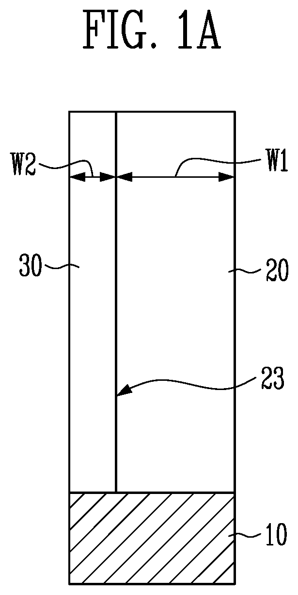
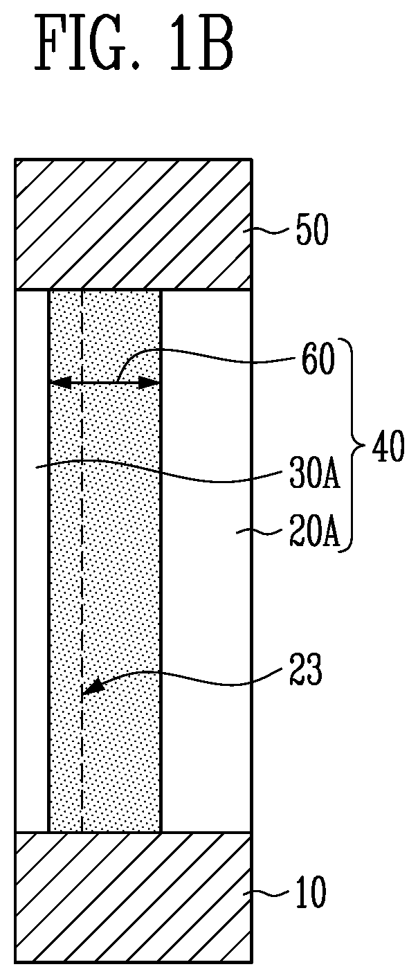
[0031]FIGS. 1A and 1B are sectional views schematically illustrating a manufacturing method of a variable resistance memory device in accordance with an embodiment of the present disclosure.
[0032]Referring to FIG. 1A, in order to form a variable resistance memory device, a first layer 20 and a...
PUM
 Abstract
Description
Claims
Application Information