Pixel Sensing Apparatus and Panel Driving Apparatus

a pixel sensing and panel technology, applied in the direction of instruments, static indicating devices, etc., can solve the problems of image quality degradation, noise influence in connection with pixel characteristic sensing, and image quality degradation, so as to reduce noise influence, reduce noise influence, and minimize noise

Active Publication Date: 2022-05-19
LX SEMICON CO LTD
View PDF1 Cites 0 Cited by
  • Summary
  • Abstract
  • Description
  • Claims
  • Application Information

AI Technical Summary

Benefits of technology

[0017]As described above, according to the present embodiment, pixel characteristics can be sensed while minimizing the influence of noise. In addition, according to the present embodiment, the influence of noise can be reduced when sensing pixel characteristics during a relative short time section. In addition, according to the present embodiment, the accuracy of sensing can be improved when sensing pixel characteristics during a relative long time section. In addition, according to the present embodiment, the influence of noise and the accuracy of sensing can be adjusted according to the length of a sensing section.

Problems solved by technology

If the source driver fails to consider such changes in the characteristics of pixels, there may occur a problem in that the pixels, when driven, exhibit undesired brightness, and the image quality is degraded.
If the source driver supplies a data voltage without considering changed characteristics of pixels, there occurs a problem of degraded image quality (for example, a blurry screen).
However, the influence of noise may become heavier in connection with pixel characteristic sensing because the latter time section is relatively longer, and the former time section is relatively shorter.
Heavy noise influence causes errors in sensing values, and the compensation process may adversely increase pixel deviations.
This may cause a problem of degraded image quality.

Method used


Image

  • Pixel Sensing Apparatus and Panel Driving Apparatus
  • Pixel Sensing Apparatus and Panel Driving Apparatus
  • Pixel Sensing Apparatus and Panel Driving Apparatus

Examples


Embodiment Construction

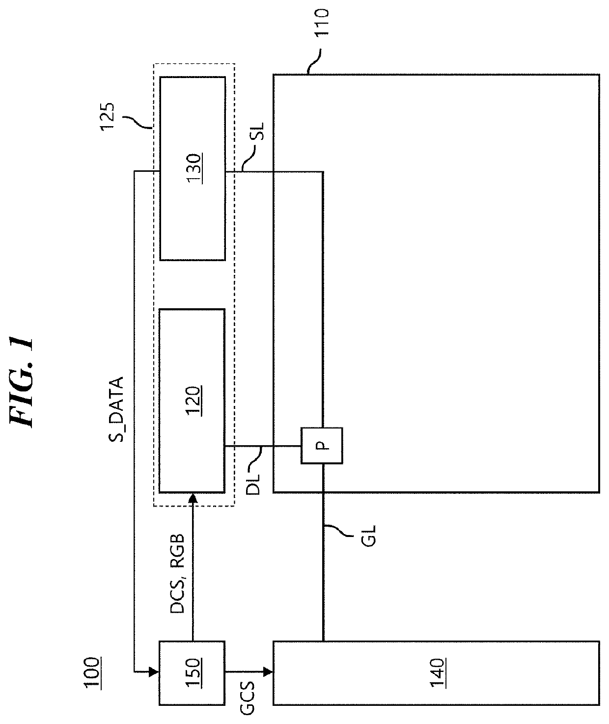
[0025]FIG. 1 is a configuration diagram of a display device according to an embodiment.

[0026]Referring to FIG. 1, the display device 100 may include a panel 110 and a panel driving devices 120, 130, 140, and 150 that drive the panel 110.

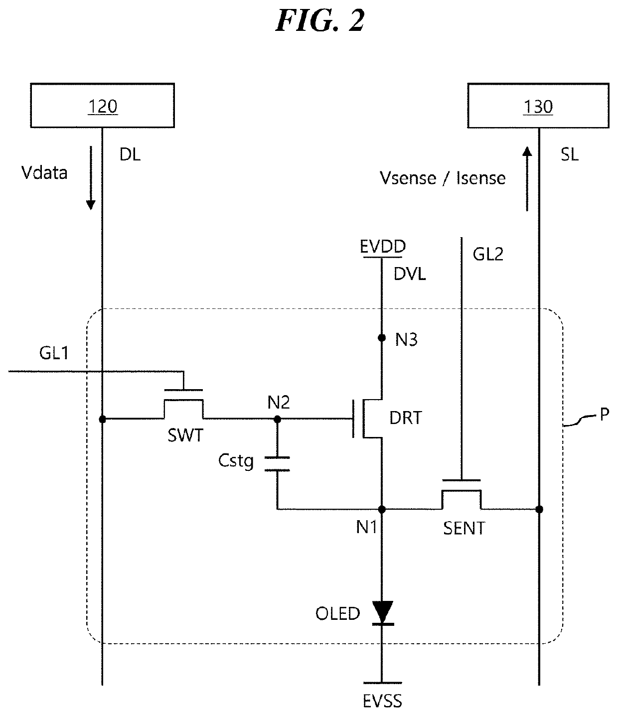
[0027]A plurality of data lines DL, a plurality of gate lines GL, and a plurality of sensing lines SL may be disposed on the panel 110, and a plurality of pixels P may be disposed on the panel 110.

[0028]The devices 120, 130, 140, and 150 that drive at least one component included in the panel 110 may be referred to as panel driving devices. For example, the data driving circuit 120, the pixel sensing circuit 130, the gate driving circuit 140, the data processing circuit 150 may be referred to as panel driving devices.

[0029]Each of the above-described circuits 120, 130, 140, and 150 may be referred to as a panel driving device, and all or a plurality of circuits may be referred to as panel driving devices.

[0030]In the panel driving devices, the gate d...


PUM


Abstract

The present embodiment relates to a technology for driving a display device, and provides a technology for adjusting the full-scale range (FSR) of an analog-to-digital converter according to a mode when sensing a pixel.

Description

CROSS REFERENCE TO RELATED APPLICATION[0001]This application claims priority from Republic of Korea Patent Application No. 10-2020-0155074, filed on Nov. 19, 2020, which is hereby incorporated by reference in its entirety.BACKGROUND1. Field of Technology[0002]The present embodiment relates to a technology for driving a display device.2. Description of the Prior Art[0003]A display device includes a source driver for driving pixels disposed on a panel.[0004]The source driver determines a data voltage according to image data, and supplies the data voltage to pixels, thereby controlling the brightness of each pixel.[0005]Meanwhile, even if the same data voltage is supplied, the brightness of each pixel may vary depending on the characteristics of the pixels. For example, a pixel includes a driving transistor, and if the threshold voltage of the driving transistor changes, the brightness of the pixel varies even if the same data voltage is supplied thereto. If the source driver fails to ...

Claims


Application Information

Patent Timeline
Patent Type & Authority Applications(United States)
IPC IPC(8): G09G3/3291G09G3/3258
CPCG09G3/3291G09G2310/0294G09G3/3258G09G3/006G09G3/3233G09G2320/045G09G2330/026G09G2330/027G09G2330/028G09G3/3225G09G2300/0828G09G2320/02
Inventor KIM, SEONG GEONKIM, WONKIM, YOUNG BOK
Owner LX SEMICON CO LTD
Why Eureka
Try Eureka