Phase Clock Generator

a generator and phase clock technology, applied in the direction of generating/distributing signals, pulse techniques, instruments, etc., can solve the problems of increasing the power consumption of the device, difficult to minimize the chip size of the vco, and easy to affect the oscillating operation

Inactive Publication Date: 2009-03-19
DONGBU HITEK CO LTD
View PDF4 Cites 0 Cited by
  • Summary
  • Abstract
  • Description
  • Claims
  • Application Information

AI Technical Summary

Benefits of technology

[0023]Embodiments of the present invention can provide a phase clock generator for use in a voltage controlled oscillator (VCO). An embodiment of the present inven

Problems solved by technology

However, since an inductor L for the LC tank circuit is a distributed element having a large size and is not manufactured through a semiconductor fabricating process, it can be difficult to minimize a chip for the VCO.
In addition, an oscillating operation may be easily affected by the matching between the inductor (L) and a capacitor (C) of the LC circuit.
However, this may increase the power consumption of the device.
However, the number of inverters connected to a transistor may be restricted.
When an oscillation period is densely set, the rising edge may be erroneously detected.
In addition, an edge detection time must be greatly increased due to the load of the memory cell A. This increased detection time may cause an err

Method used


Image

  • Phase Clock Generator
  • Phase Clock Generator
  • Phase Clock Generator

Examples


Embodiment Construction

[0038]Embodiments of a phase clock generator will be described in detail with reference to accompanying drawings.

[0039]FIG. 7 is a block diagram schematically showing components of a voltage controlled oscillator (VCO) 100 according to an embodiment of the present invention.

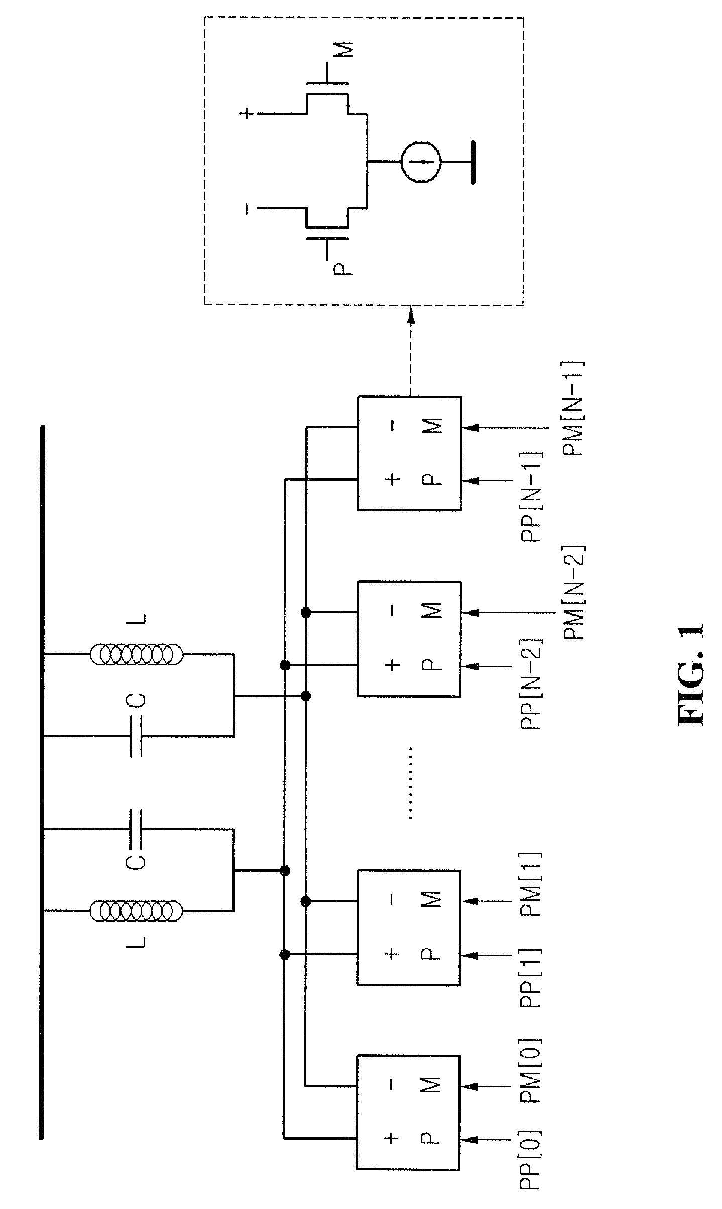
[0040]Referring to FIG. 7, a VCO 100 according to an embodiment can include a delay locked loop 110 and a phase clock generator 200. The DLL 110 can include a phase detector 112, a charge pump 114, a loop filter 116, and a voltage controlled delay line (VCDL) 118.

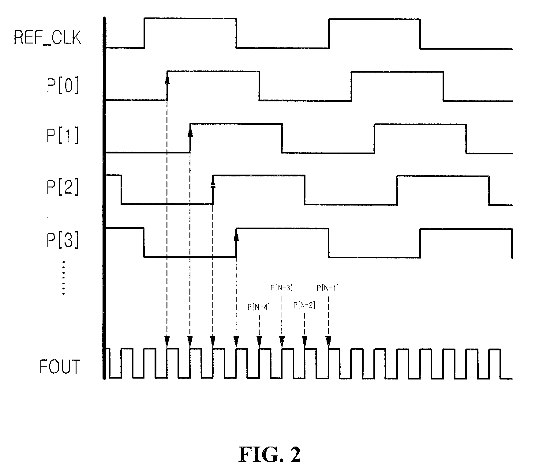
[0041]The VCDL 118 can receive a reference clock (REF_CLK) from an oscillating circuit, and generates a plurality of phase-delayed signals (P[0] to P[N−1]) by phase-delaying the reference clock. The oscillating circuit can be, for example, a temperature controlled X-tal oscillator (TCXO).

[0042]The phase detector 112 can sequentially receive the phase-delayed signals from the VCDL 118 and then compares the phase-delayed signals with the reference clock to...


PUM


Abstract

Disclosed is a phase clock generator. The phase clock generator can include transistors and a buffer. The transistors are connected between a power line and a grounding line and are provided in a form of a 4×N matrix to receive a plurality of phase-delayed signals through their gate terminals. Four transistors can form a unit column between the power line and the grounding line. From ground line to power line, the first two transistors of the unit column provide a pair of NMOS transistors, and the second two transistors provide a pair of PMOS transistors. The buffer is connected to a line, which is provided between the pair of the NMOS transistors and the pair of the PMOS transistors forming the unit column, to transmit a clock signal.

Description

CROSS-REFERENCE TO RELATED APPLICATION[0001]The present application claims the benefit under 35 U.S.C. § 119 of Korean Patent Application No. 10-2007-0093431, filed Sep. 14, 2007, which is hereby incorporated by reference in its entirety.BACKGROUND[0002]Recently, various narrow band and broad band communication systems have been developed to provide services, such as mobile communications, satellite communications, and broadcasting. Circuits constituting the communication systems, including a mixer, a balloon circuit, a modulator, and a demodulator, require a clock signal in order to process frequency signals having various channels.[0003]FIG. 1 is a circuit diagram schematically showing components of an edge combiner for a voltage controlled oscillator (VCO), and FIG. 2 is a timing chart showing measured output signals of the edge combiner of FIG. 1.[0004]A VCO typically includes a delayed locked loop (DLL) and an edge combiner. The DLL generates various phase signals P[0], P[1], ....

Claims


Application Information

Patent Timeline
IPC IPC(8): G06F1/04
CPCG06F7/68H03K2005/00052H03K5/13H03L7/099
Inventor KIM, TAE GYU
Owner DONGBU HITEK CO LTD
Why Eureka
Try Eureka