Chip chuck and chip supporting device for optical inspection

a chip supporting device and optical inspection technology, applied in the direction of individual semiconductor device testing, optical radiation measurement, instruments, etc., can solve the problems of not meeting the test requirements of conventional chip supporting devices and less accurate inspection results of optical characteristics

Pending Publication Date: 2022-06-02
MICROELECTRONICS TECH INC
View PDF6 Cites 0 Cited by
  • Summary
  • Abstract
  • Description
  • Claims
  • Application Information

AI Technical Summary

Benefits of technology

[0004]The present invention has been accomplished in view of the above-noted circumstances. It is an objective of the prese...

Problems solved by technology

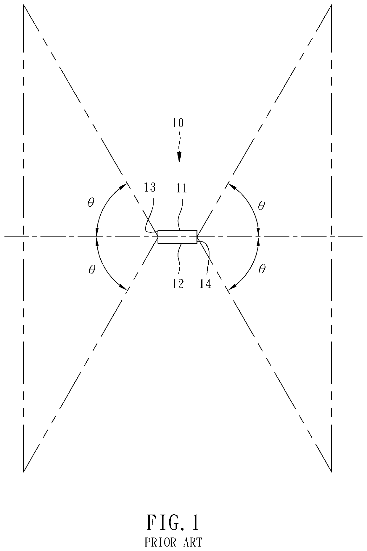
The larger the divergent angle θ, the more the interference between the light and the chip supporting device, and the less accurate the inspection results of the optical characteristics.
In addi...

Method used


Image

  • Chip chuck and chip supporting device for optical inspection
  • Chip chuck and chip supporting device for optical inspection
  • Chip chuck and chip supporting device for optical inspection

Examples


Embodiment Construction

[0025]First of all, it is to be mentioned that same or similar reference numerals used in the following embodiments and the appendix drawings designate same or similar elements or the structural features thereof throughout the specification for the purpose of concise illustration of the present invention. It should be noticed that for the convenience of illustration, the components and the structure shown in the figures are not drawn according to the real scale and amount, and the features mentioned in each embodiment can be applied in the other embodiments if the application is possible in practice. Besides, when it is mentioned that an element is disposed on another element, it means that the former element is directly disposed on the latter element, or the former element is indirectly disposed on the latter element through one or more other elements between aforesaid former and latter elements. When it is mentioned that an element is directly disposed on another element, it means...


PUM


Abstract

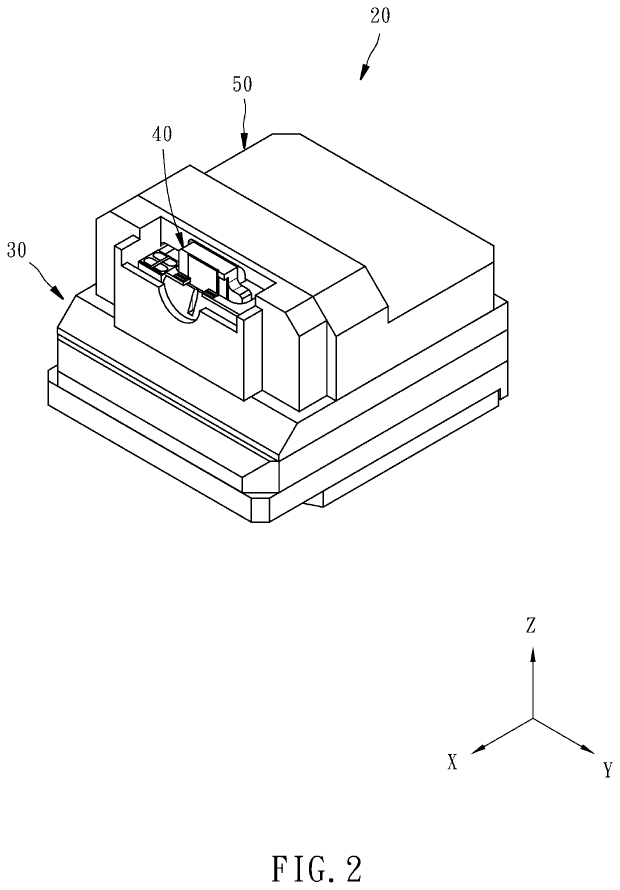
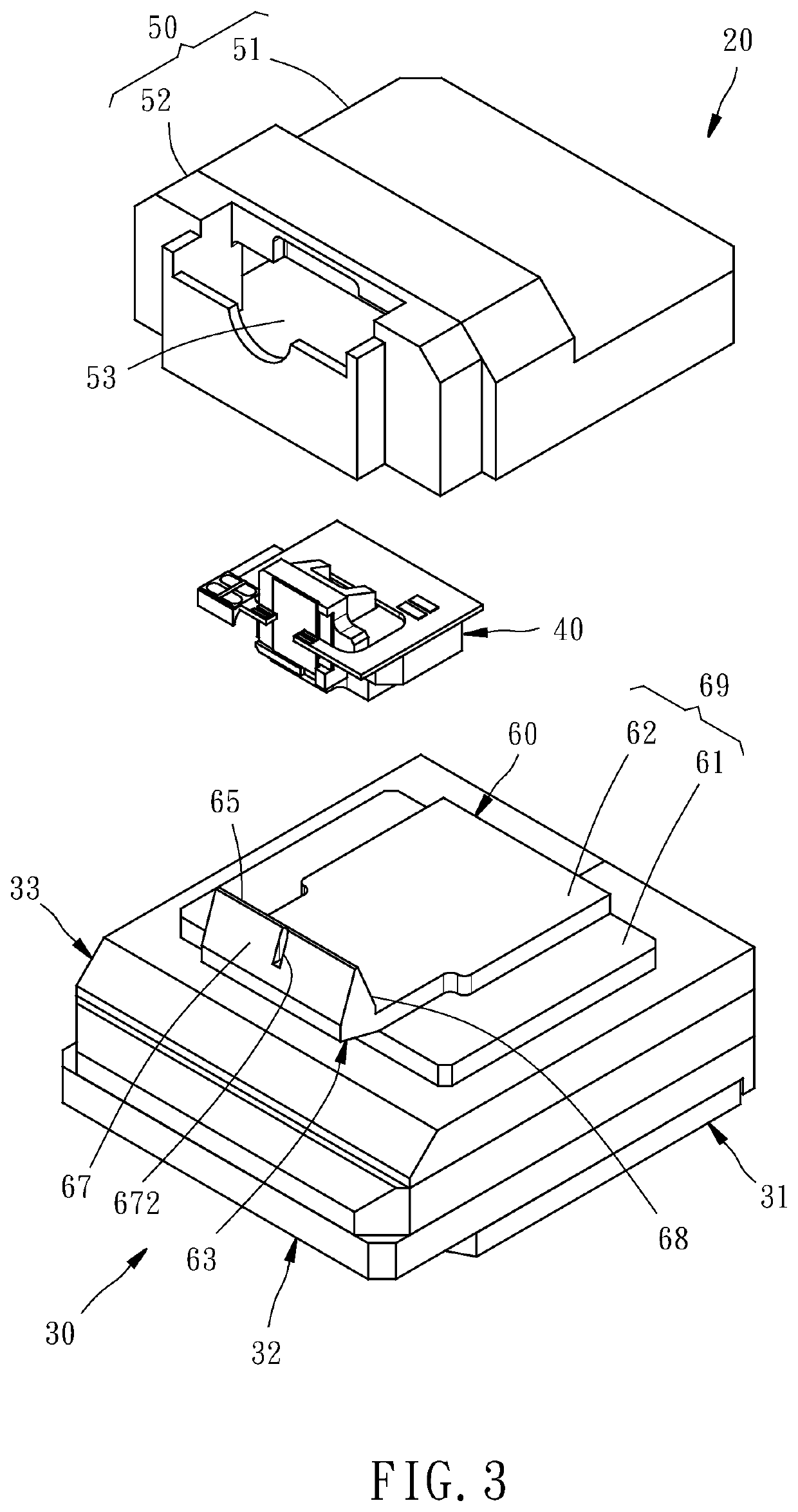
A chip chuck includes front and back slopes obliquely extending toward a bottom surface from front and back edges of a top surface having a chip placement area for supporting a chip under test, and is defined with an imaginary vertical reference line perpendicular to the chip placement area and an imaginary horizontal reference line. The front and back slopes are connected with the chip placement area and each provided with an included acute angle with respect to the imaginary horizontal reference line, thereby avoiding interference with light emitted from the chip. A chip supporting device includes a chip chuck, and an optical sensing module fixed relative thereto and including an optical sensor whose light receiving surface faces toward a back light emitting surface of the chip, thereby enabling optical characteristic inspection of front and back light emitting surfaces of the chip at the same time.

Description

BACKGROUND OF THE INVENTION1. Field of the Invention[0001]The present invention relates generally to optical inspection equipment for light emitting chips and more particularly, to a chip chuck for optical inspection, and a chip supporting device including the chip chuck.2. Description of the Related Art[0002]Referring to FIG. 1, a light emitting chip 10 (hereinafter also referred to “chip under test”) is shown. The light emitting chip 10 is provided on a top surface 11 or a bottom surface 12 thereof with conductive contacts (not shown), or may be provided on both the top and bottom surfaces 11 and 12 with conductive contacts. When the conductive contacts are electrified, the light emitting chip 10 emits light from two sides thereof, thereby having two opposite lateral light emitting surfaces. That means a front light emitting surface 13 (front facet) and a back light emitting surface 14 (back facet) of the light emitting chip 10 both emit light. The scope of luminescence is shown b...

Claims


Application Information

Patent Timeline
IPC IPC(8): G01J1/02G01R31/26
CPCG01J1/0223G01J2001/4252G01R31/2635G01J1/0403G01J1/0252G01R1/0466
Inventor LIN, HUNG-ILEE, BO-SIANCHEN, YI-HUNG
Owner MICROELECTRONICS TECH INC
Why Eureka
Try Eureka