LED display

a technology of led display and micro light-emitting diodes, which is applied in the field of display, can solve the problems of large amount of contact points to be handled, difficult to transfer such a large amount of micro light-emitting diodes to conventional machines, etc., and achieve the effect of high-solution display and low cos

Pending Publication Date: 2022-07-21
INNOSERV +1
View PDF37 Cites 0 Cited by
  • Summary
  • Abstract
  • Description
  • Claims
  • Application Information

AI Technical Summary

Benefits of technology

[0008]It is the primary objective of the present invention to provide an inexpensive and high-solution display.

Problems solved by technology

In the making of micro light-emitting diodes, problems are encountered.
Transfer of such a large amount of micro light-emitting diodes is too difficult for conventional machines that are suitable for making average light-emitting diodes.
Moreover, an even larger amount of contact points have to be handled to attach such a large amount of micro light-emitting diodes to a circuit board.
Such complicated wiring required a precise and expansive process and are not good for the transfer of such a large amount of micro light-emitting diodes.
Hence, the rate of defects in the making of the displays equipped with micro light-emitting diodes is high.

Method used


Image

  • LED display
  • LED display
  • LED display

Examples


Embodiment Construction

[0020]Referring to FIGS. 1 through 7, a display 10 includes at least one circuit board 20 and at least one group of micro light-emitting diodes 39 according to the preferred embodiment of the present invention.

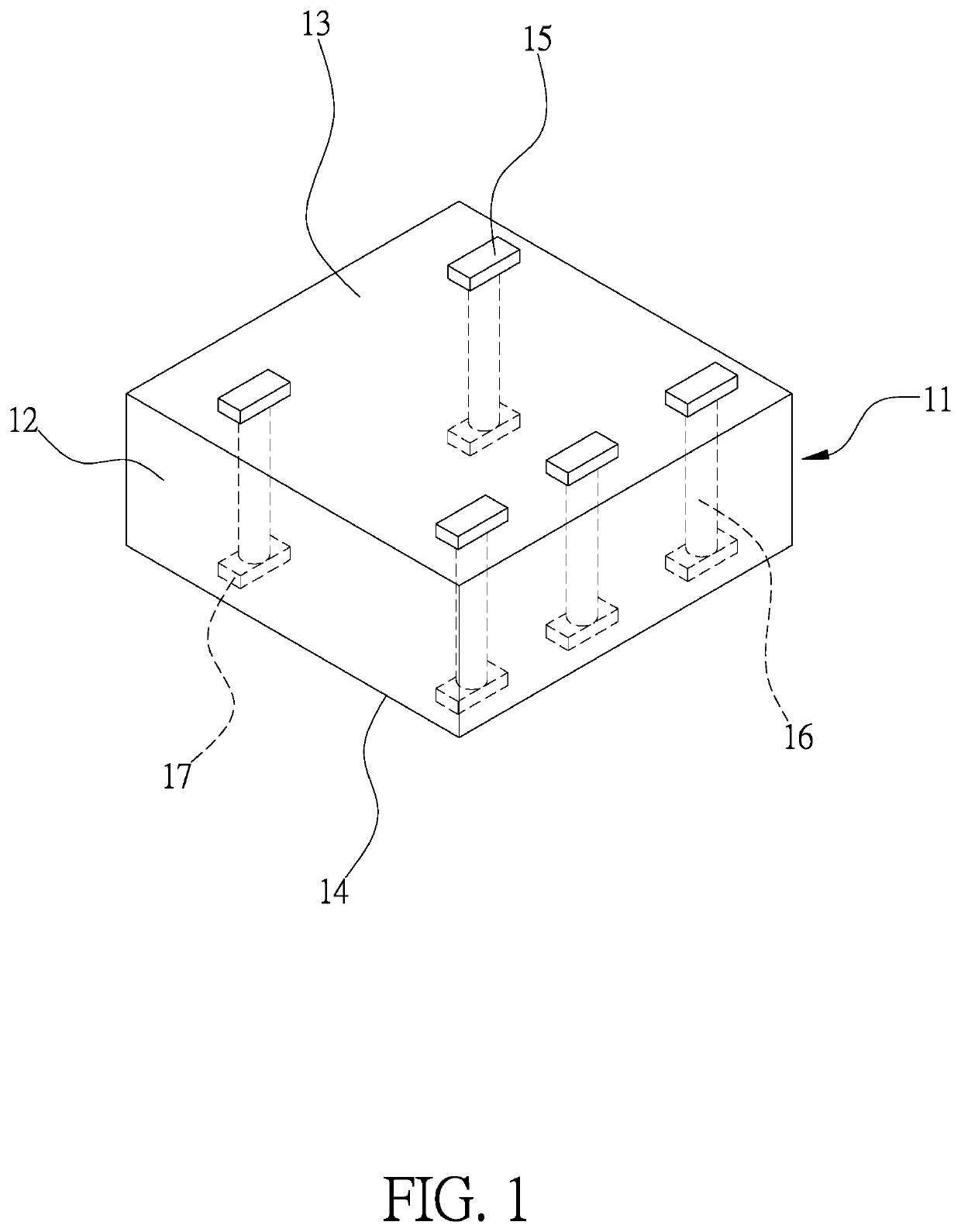
[0021]Referring to FIG. 1, a driver integrated circuit (“IC”) 11 includes a base 12 formed with two opposite faces 13 and 14. There are bonding pads 15 on the face 13 of the base 12. There are bonding pads 17 on the face 14 of the base 12. The bonding pads 17 are shaped and located corresponding to the bonding pads 15. A through-silicon via (“TSV”) technique is used to make conductors 16 in the base 12. Each of the conductors 16 connects a corresponding one of the bonding pads 15 to a corresponding one of the bonding pads 17. Thus, the faces 13 and 14 of the base 12 of the driver IC 11 are electrically connected to each other.

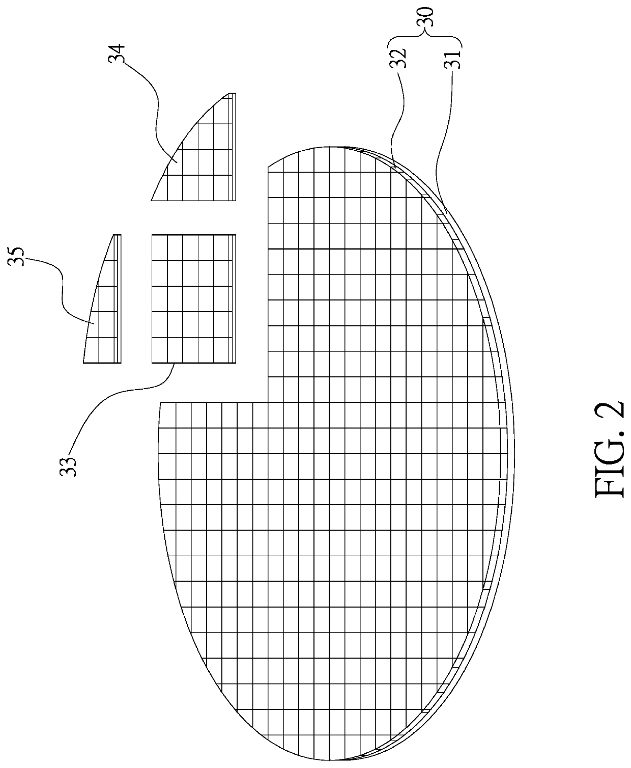
[0022]Referring to FIG. 2, an original substrate 30 includes a crystal layer 31 of sapphire for example grown on an extensive layer 32 by an epitaxy tech...


PUM

PropertyMeasurementUnit
electricallyaaaaaaaaaa
defectsaaaaaaaaaa
solutionaaaaaaaaaa

Abstract

A display includes micro LEDs connected to a color conversion layer and driver ICs connected to the micro LEDs via an electrically connecting layer. Each micro LEDs includes an N pad and a P pad. The micro LEDs emit light of a same color, and the color conversion layer converts the light into various colors. The electrically connecting layer includes elongated negative electrodes connected to the N pads and elongated positive electrodes connected to the P pads. Each driver IC includes a first group of bonding pads on a face, a second group of bonding pads on an opposite face, and conductors for connecting the first group of bonding pads to the second group of bonding pads. Each bonding pad in the first group is connected to an elongated negative or positive electrode. The circuit board is connected to the second group of bonding pads of each driver IC.

Description

BACKGROUND OF INVENTION1. Field of Invention[0001]The present invention relates to a display and, more particularly, to an LED display.2. Related Prior Art[0002]A light-emitting diode (“LED”) display includes light-emitting diodes attached to a substrate by glue. Each of the light-emitting diodes is in the form of a die cut from a wafer. The attachment of the light-emitting diodes to the substrate is called “die bonding.”[0003]A light-emitting diode in the form of a flip chip includes a positive electrode P and a negative electrode N on a same side, and each of the positive and negative electrodes is covered by a block of solder. The light-emitting diode in the form of a flip chip is cut and bonded before it can be electrically connected to a circuit board.[0004]Pixels-per-inch (“PPI”) is often used to describe the resolution of a display. However, the size of a micro light-emitting diode is smaller than 100 μm, about 1% of the size of a regular light-emitting diode. In the making o...

Claims


Application Information

Patent Timeline
Patent Type & Authority Applications(United States)
IPC IPC(8): H01L33/62H01L27/15H01L33/08H01L33/38H01L33/48
CPCH01L33/62H01L27/156H01L33/486H01L33/38H01L33/08H01L25/167H01L25/0753H01L33/0093H01L33/504
Inventor WU, MENG-CHIHTIEN, CHIEN-KUOLIN, CHUN-CHUNG
Owner INNOSERV
Why Eureka
Try Eureka