Semiconductor wafer testing apparatus with a combined wafer alignment/wafer recognition station

a technology of combined wafer alignment and recognition station, which is applied in the direction of instruments, charge manipulation, furnaces, etc., can solve the problem of a lot of time required for the overall processing

Inactive Publication Date: 2000-02-22
SAMSUNG ELECTRONICS CO LTD
View PDF14 Cites 20 Cited by
  • Summary
  • Abstract
  • Description
  • Claims
  • Application Information

AI Technical Summary

Problems solved by technology

During this processing, as the operator looks closely at the wafer to see its code, contamination from the operator may be generated as well as particulate dust due ...

Method used


Image

  • Semiconductor wafer testing apparatus with a combined wafer alignment/wafer recognition station
  • Semiconductor wafer testing apparatus with a combined wafer alignment/wafer recognition station
  • Semiconductor wafer testing apparatus with a combined wafer alignment/wafer recognition station

Examples


Embodiment Construction

Reference will now be made in detail to a preferred embodiment of the present invention, examples of which are illustrated in the accompanying drawings.

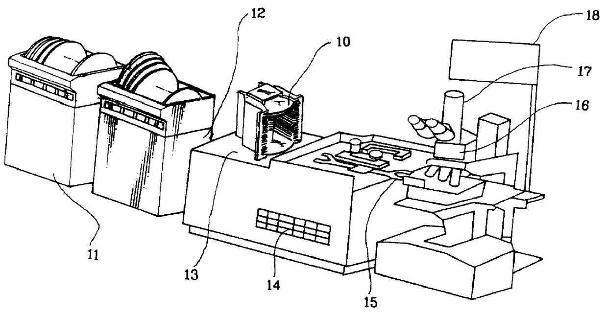
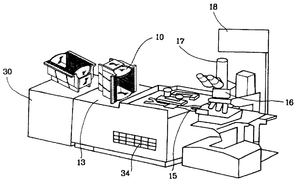
Referring to FIG. 3, the inventive semiconductor wafer testing apparatus includes an autoloader 15 which is a robot arm, a microscope 16, a microscope camera 17, a monitor 18 and a controller 34. This apparatus is substantially similar to the conventional elements having like or similar references numerals as shown in FIG. 1.

However, as shown in FIGS. 3 through 6, the testing apparatus of this preferred embodiment has one work table 30 having an opening therein in which a flat zone aligner 51 and an optical character recognizer 61 are both provided for movement into and out of the table opening; while the conventional testing apparatus requires one work table 11 for wafer alignment and a separate table on which an identification (ID) finder 12 is installed.

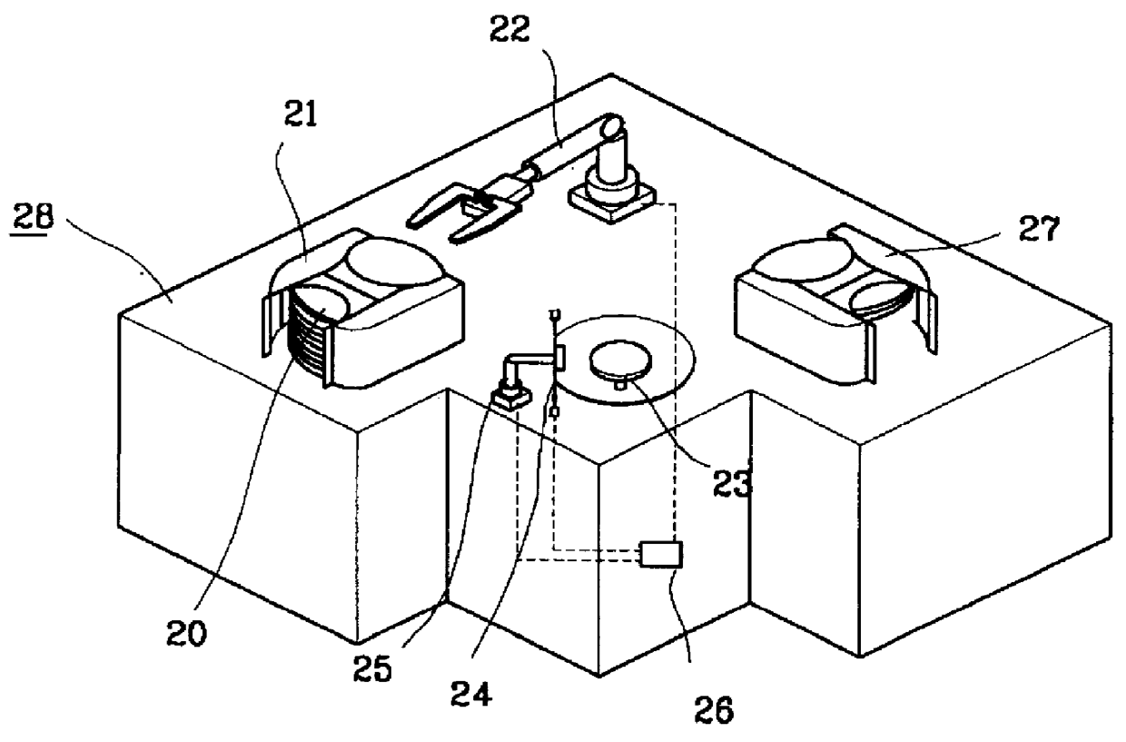
According to the inventive semiconductor wafer testing apparatus, wafers on th...


PUM


Abstract

A semiconductor wafer testing apparatus has a work table on which a carrier containing semiconductor wafers to be checked is placed. The work table is equipped for combined wafer alignment and wafer code recognition while the wafers remain in their carrier in one position on the work table. The alignment is accomplished with a wafer flat zone aligner which has a pair of roller pins each coming in contact with circumferences of the wafers being stacked in the carrier through an open lower part of the carrier and an opening in the table. The wafer code recognition is accomplished with an optical character recognizer that moves up and down and forward and backward with respect to the carrier, and interposes between the wafers in the carrier so as to read out codes which are on each wafer. This combined automated work station helps prevent contamination of the wafers by an operator or by unnecessary handling of the wafers, and also reduces cycle time for the entire inspection process.

Description

1. Field of the InventionThe present invention relates generally to a semiconductor wafer testing apparatus. More particularly, it relates to an improved semiconductor wafer testing apparatus which has an automated station in which both wafer alignment and wafer recognition are performed under automatic control before a wafer test, without having to move the wafers to two separate stations.2. Background of the Related ArtFor each step in semiconductor device fabrication, a testing apparatus is used to inspect and measure the devices upon completion of the corresponding process. Generally, one wafer that has already undergone a prescribed process of fabrication is preselected to be placed under sampling inspection in the semiconductor wafer testing apparatus.The sampling inspection procedure of the conventional wafer testing apparatus is now described with reference to FIG. 1.The sampling inspection begins with loading a carrier full of semiconductor wafers which have undergone a pre...

Claims


Application Information

Patent Timeline
IPC IPC(8): G01R31/28H01L21/00B65G49/07H01L21/66H01L21/677H01L21/68
CPCG01R31/2831H01L21/67271Y10S269/903Y10S414/137Y10S414/136Y10S414/14H01L22/00
Inventor KIM, YU KWEONKIM, DONG HO
Owner SAMSUNG ELECTRONICS CO LTD
Why Eureka
Try Eureka