Test method of one chip micro-computer and one chip micro-computer for conducting the test

a chip microcomputer and test method technology, applied in the direction of unauthorized memory use protection, instruments, error detection/correction, etc., can solve the problems of third parties wrongly reading written data, complicated or difficult procedures for reading written data, and the possibility of third parties wrongly reading data

Inactive Publication Date: 2000-06-27
KAWASAKI MICROELECTRONICS
View PDF7 Cites 15 Cited by
  • Summary
  • Abstract
  • Description
  • Claims
  • Application Information

AI Technical Summary

Benefits of technology

Moreover, according to the second invention of the present application, the data conversion operating circuit includes a circuit for non-degenerate converting the command code by conducting an EXCLUSIVE-OR operation between the command code and the test conversion data, thereby making it possible to conduct the non-regenerate conversion with a relatively simple circuit configuration.

Problems solved by technology

However, if this function is given, there is a possibility that a third party wrongfully reads the written data.
(A2) Procedures for reading written data are made to be complex or difficult so as to reduce the possibility for any third party to wrongfully read the data.
As regards A1, even if there is a suspicion that written data in the installed ROM is defective after shipment, it has a fatal disadvantage in that another ROM test cannot be conducted once the non-reversible physical modification has been made.
Furthermore, due to the necessity of special processing of a non-reversible physical modification such as the disconnection of a security fuse after a shipping test, test costs are disadvantageously increased.
This is particularly disadvantageous to ASIC (or Application Specific Integrated Circuits) having many types but with small amounts.
There is thus a limit to the security; i.e., the prevention of wrongful reading by the third party.
Normally, so many terminals cannot be used for setting a ROM test mode and therefore a combination of so many input values cannot be conditioned.
Moreover, to improve the security to prevent the wrongfully reading and to ensure the defense against it, a lot of terminals, pins and components are required, resulting in a cost hike.
Moreover, the prior art A2 has a disadvantage to, for example, MCUs having the same hardware configuration but different from one another in data written in installed ROMs in accordance with purposes of parties who make orders.
In this case, the fact that procedures of reading written data in the installed ROMs are the same makes it disadvantageously possible that persons responsible for orders wrongfully read data written in the installed ROMs of others.
That is, it is feared that the security mechanism of the MCU is revealed to a lot of users, with the result that it virtually loses its value.
As regards A3, it has a disadvantage in that there is a limit to test methods and there is a chance that check sums or the like coincide with one another.
To realize it, however, many components are required and costs increase greatly.
Furthermore, only the judge results of whether or not defective data exists are outputted to the outside of the MCU and it is impossible to know which written data is defective in the installed ROM or the like.
This makes failure analysis disadvantageously difficult.
As regards A4 and A5, it has a disadvantage in that the permission key for reading out the data in the EPROM cell array or setting a single chip mode comprises only one or several byte.
Therefore, security against wrongful read out may not be enough.
As a result, the program, for example, malfunctions and an expected operation cannot be observed, thereby making it possible to discriminate failure.
This comparison example has, however, a disadvantage in that costs increase due to the incorporation of the ROM test program or in that the address area a user can use is narrowed.
In addition, it has a critical problem that, since the test program is incorporated, it is feared that the third party wrongfully reads written data once he or she discovers at which address the test program starts.
It is difficult for persons who order MCUs having the same hardware configuration but different written data in the ROM installed to keep individual written data confident.

Method used


Image

  • Test method of one chip micro-computer and one chip micro-computer for conducting the test
  • Test method of one chip micro-computer and one chip micro-computer for conducting the test
  • Test method of one chip micro-computer and one chip micro-computer for conducting the test

Examples


first embodiment

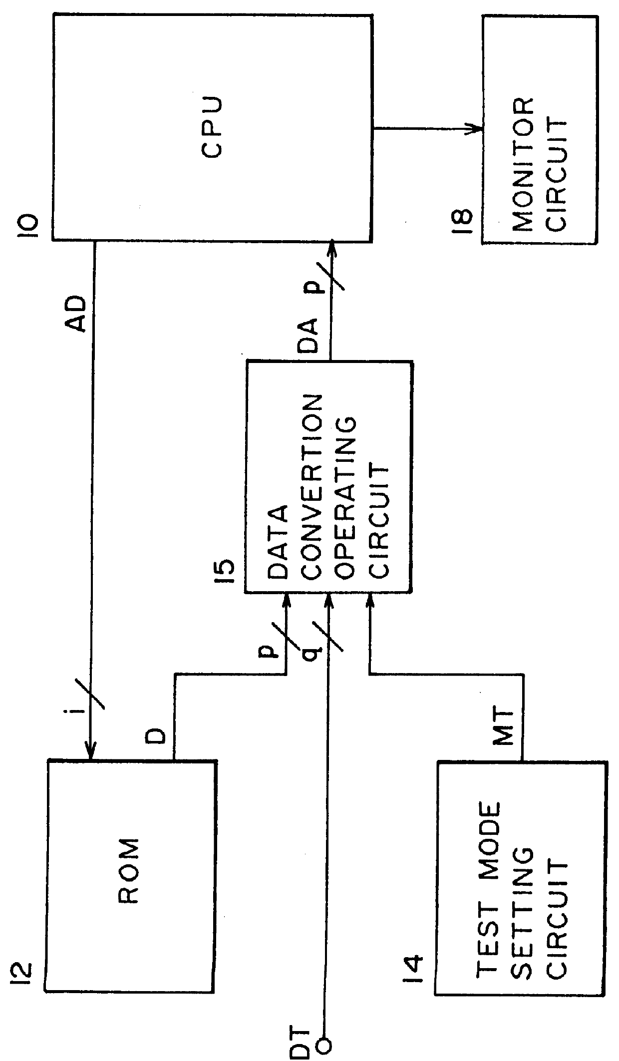
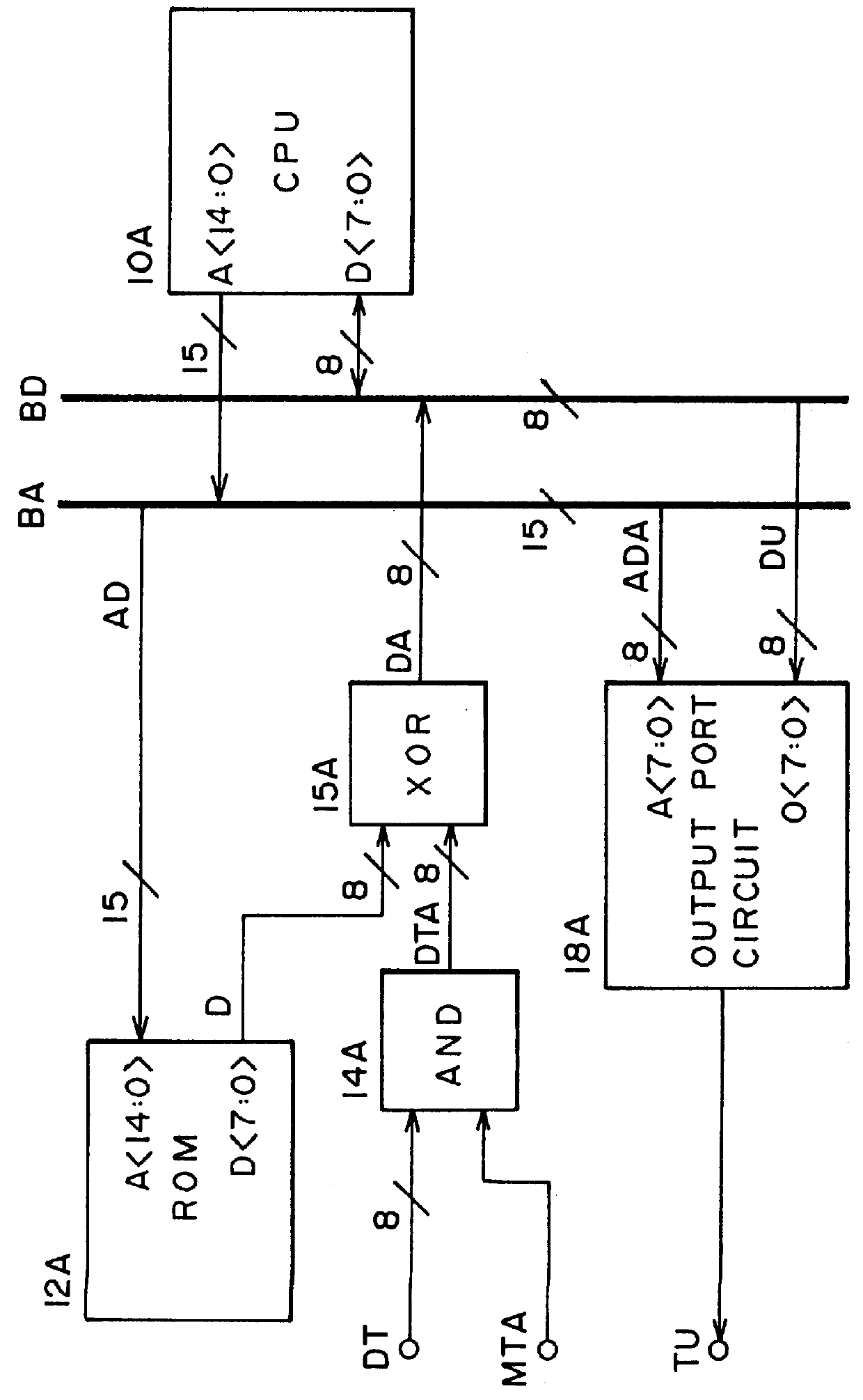
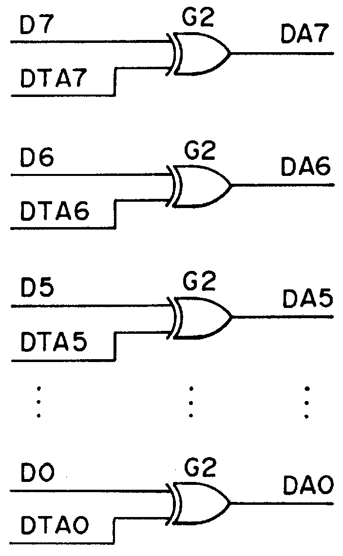
FIG. 2 is a block diagram showing the structure of the MCU to which the present invention is applied.

In this embodiment, a one-chip microcomputer is used as the MCU. As shown in FIG. 2, the MCU comprises a CPU 10A and a ROM 12A. Data written in the ROM 12A includes a program for a command code of the CPU 10A. The command code is executed by the CPU 10A through an address bus BA and a data bus BD. In addition, in this embodiment, the ROM test is aimed at testing the content of the data written in the ROM 12A.

In this embodiment, the MCU further comprises a test mode setting circuit 14A, a data conversion operating circuit 15A and an output port circuit 18A to conduct the ROM test.

A test mode signal MTA is inputted from the outside of the MCU into the test mode setting circuit 14A. The test mode signal MTA is in an H state in the ROM test mode and in an L state in the normal operation mode.

It is noted that the test mode signal MTA can be generated within the MCU. For example, it is pos...

second embodiment

FIG. 5 is a block diagram showing the structure of the MCU to which the present invention is applied.

As shown in FIG. 5, the MCU is provided with a RAM 22, a timer 24 and an interrupt circuit 26 in addition to the MCU of the first embodiment. The MCU is further provided with a block test mode setting circuit 20. This block test mode setting circuit 20 individually controls valid or invalid of operation of the CPU 10A, the RAM 22, the timer 24 and the interrupt circuit 26.

In this embodiment, predetermined data can be written (or downloaded) into desired address of the RAM 22 by the data DT from the outside of the MCU according to the present invention. The program thus downloaded into the RAM 22 can perform various operations. Downloading of the program (hereinafter referred to as "external program downloading") is one embodiment of the present invention.

According to the above external program downloading, tests of the RAM 22, the ROM 12A and peripheral functions of the timer 24 and ...


PUM

PropertyMeasurementUnit
DAaaaaaaaaaa
bit lengthaaaaaaaaaa
forceaaaaaaaaaa

Abstract

When testing internal state of one chip micro-computer having a CPU and a ROM installed in a single package, data D read from the ROM is subjected to non-degenerate conversion using data DT from the outside and is executed as a command code by the CPU in a test mode. To input the data DT which can serve as a correct command code from the outside, it is necessary that the data D is known. A third party is incapable of conducting a test for testing the internal state and wrongfully reading the written data.

Description

1. Field of the InventionThe present invention relates to a test method of one chip micro-computer for testing internal state of the one chip micro-computer having at least a CPU and a ROM installed in a single package, the ROM connected to the CPU such that the written data of the ROM can be executed by the CPU as a command code, and relates to one chip micro-computer for conducting the test. More particularly, the present invention relates to a test method of one chip micro-computer capable of testing (including a ROM test), no matter when, the internal state of one chip micro-computer which is the target of the present invention while preventing the third party from wrongfully reading the data of the ROM only by adding relatively simple circuits.2. Description of the Related ArtConventionally, there has been provided one chip micro-computer (to be referred to as MCU (Micro Controller Unit) hereinafter) having a CPU and a ROM (Read Only Memory), connected to the CPU such that the ...

Claims


Application Information

Patent Timeline
Patent Type & Authority Patents(United States)
IPC IPC(8): G06F11/273G06F11/263G06F12/14
CPCG06F11/263G06F11/2635G06F12/1408
Inventor YAMADA, YASUO
Owner KAWASAKI MICROELECTRONICS
Why Eureka
Try Eureka