Piezoelectric/electrostrictive element

a technology of electro-electrostrictive elements and piezoelectrics, applied in piezoelectric/electrostrictive/magneto-strictive devices, identification means, instruments, etc., can solve the problems of large generated force, small amount, and quick response speed

Inactive Publication Date: 2000-07-18
NGK INSULATORS LTD
View PDF25 Cites 62 Cited by
  • Summary
  • Abstract
  • Description
  • Claims
  • Application Information

AI Technical Summary

Problems solved by technology

Moreover, the response speed is quick, and the generated force is large.
It is feared, for example, that the displacement amount may be small when the element is utilized for actuators based on the inverse piezoelectric effect, and the sensitivity may be low when the element is utilized for sensors based on the piezoelectric effect.
Therefore, there is a possibility that when the piezoelectric / electrostrictive element is utilized for actuators, the control thereof may become difficult.
When the piezoelectric / electrostrictive element is utilized for sensors, it is necessary to connect, at a downstream position thereof, an expensive amplifier having a large amplification factor provided with a considered noise suppression performance.
It is feared that the problems as described above may be extremely disadvantageous especially in the case of production of electronic instruments in each of which a large number of main piezoelectric / electrostrictive elements are used, and it is necessary to maintain a constant quality of each of the piezoelectric / electrostrictive elements, for example, in the case of production of display devices each of which comprises a large number of main piezoelectric / electrostrictive elements arranged corresponding to picture elements (image pixel).
Accordingly, polarization does not proceed easily at deep portions.
Cracks appear during the phase transition in some cases.
As a result, the materials make a cause to deteriorate the element characteristics.

Method used


Image

  • Piezoelectric/electrostrictive element
  • Piezoelectric/electrostrictive element
  • Piezoelectric/electrostrictive element

Examples


Embodiment Construction

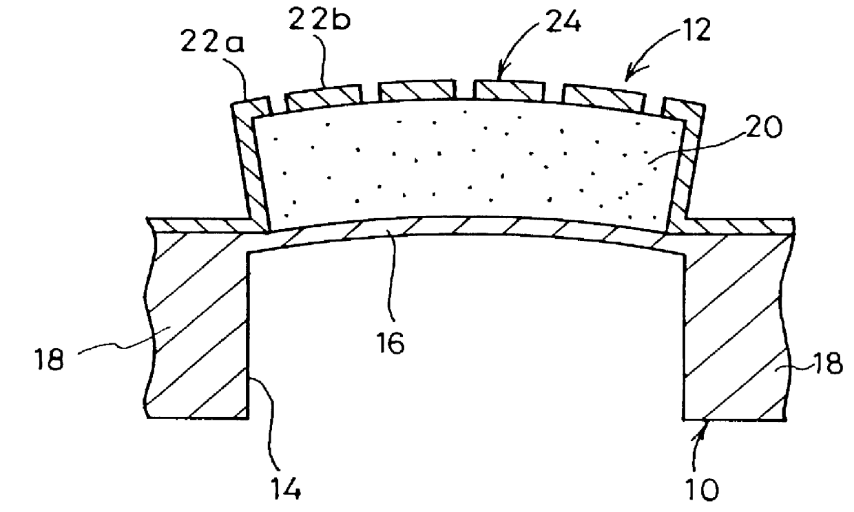
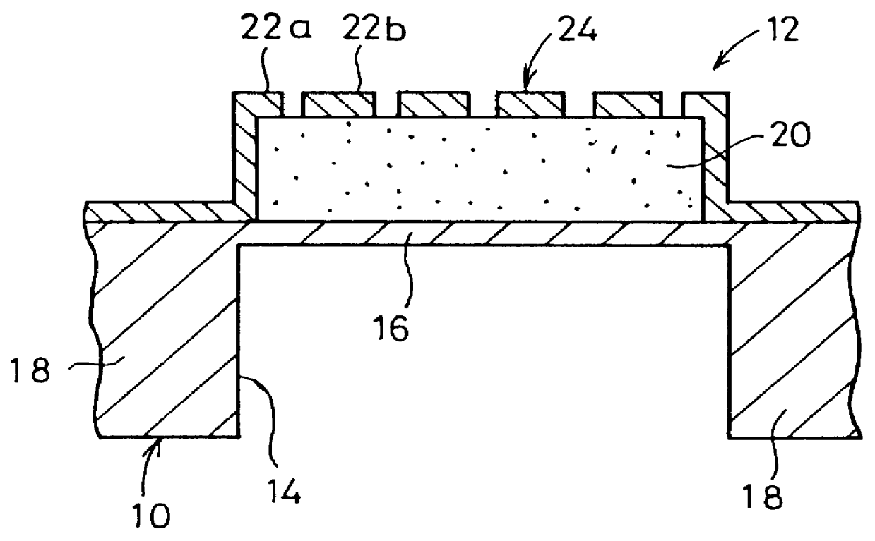
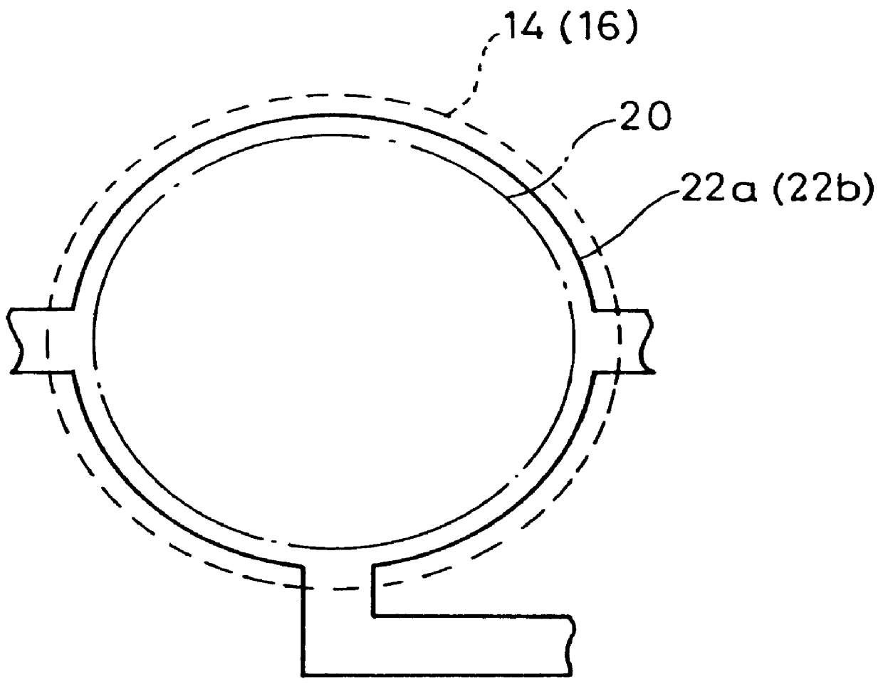
Next, explanation will be made for a display device according to a specified embodiment in which the piezoelectric / electrostrictive element according to the embodiment of the present invention is applied to the display device. Components or parts corresponding to those shown in FIG. 1 are designated by the same reference numerals, duplicate explanation of which will be omitted.

As shown in FIG. 20, the display device according to the specified embodiment comprises an optical waveguide plate 42 for introducing light 40 thereinto, and a driving unit 44 provided opposingly to the back surface of the optical waveguide plate 42 and including a large number of actuator elements 12 arranged corresponding to picture elements.

The optical waveguide plate 42 has its flat and smooth front and back surfaces, having an optical refractive index so that the light introduced into the inside is subjected to total reflection without being transmitted to the outside of the optical waveguide plate 42 thr...


PUM


Abstract

Disclosed is a piezoelectric / electrostrictive element composed of an actuator section of a uni-morph type comprising a main actuator element including a piezoelectric / electrostrictive layer and a pair of electrodes formed on a first principal surface of the piezoelectric / electrostrictive layer; a vibrating section which contacts with a second principal surface of the piezoelectric / electrostrictive layer for supporting the main actuator element; and a fixed section for supporting the vibrating section in a vibrative manner; wherein a relationship of y=ax is satisfied, and an expression of +E,fra 1 / 10+EE < / =a< / =100 is satisfied provided that x represents a distance between the pair of electrodes (1 mu m< / =x< / =200 mu m), and y represents a thickness of the piezoelectric / electrostrictive layer (1 mu m< / =y< / =100 mu m). Accordingly, it is possible to greatly increase the relative displacement amount between the no-voltage-loaded state and the voltage-applied state and the relative displacement amount between the states in which mutually opposite electric fields are applied, making it possible to realize easy control when the element is utilized for actuators and improvement in sensitivity when the element is utilized for sensors.

Description

1. Field of the InventionThe present invention relates to a piezoelectric / electrostrictive element. In particular, the present invention relates to a piezoelectric / electrostrictive element of the uni-morph type to be used, for example, for actuators, filters, displays, transformers, microphones, sounding bodies (such as speakers), various vibrators, resonators, oscillators, discriminators, gyroscopes, and sensors. The element referred to herein includes elements which convert electric energy into mechanical energy, i.e., into mechanical displacement, force, or vibration, as well as elements which perform conversion reversely from the latter to the former.2. Description of the Related ArtRecently, it has been demanded, in the fields of optics, precision manufacturing, etc., to use a displacement element for adjusting the optical path length or the position on the order of submicron, and a detecting element for detecting minute displacement after converting it into an electric variati...

Claims


Application Information

Patent Timeline
Patent Type & Authority Patents(United States)
IPC IPC(8): G02B26/08G09G3/34H01L41/09G09F9/305G09G3/20H10N30/20
CPCG02B26/08G09F9/305G09G3/3433H01L41/0973G09G3/2014G09G3/2022G09G3/3493H10N30/2047
Inventor TAKEUCHI, YUKIHISANANATAKI, TSUTOMUTAKAHASHI, MASAO
Owner NGK INSULATORS LTD
Why Eureka
Try Eureka