Optical switching device

a switching device and optical technology, applied in the field of optical switching devices, can solve the problems of small transmission change, large stack of layers required for their operation, and small contrast, and achieve the effects of simple layer structure, simple layer structure, and high ra

Inactive Publication Date: 2000-08-08
U S PHILIPS CORP
View PDF4 Cites 27 Cited by
  • Summary
  • Abstract
  • Description
  • Claims
  • Application Information

AI Technical Summary

Benefits of technology

It is an object of the present invention to provide, inter alia, an optical switching device, which can be switched more readily and at a higher rate between both states. In addition, it must be possible to perform said conversion relatively rapidly, i.e. within 0.05 s, at a common temperature and pressure. Moreover, the switching device should have a simple layer structure.

Problems solved by technology

A drawback of oxidic electrochromic devices is that an extensive stack of layers is required for their operation.
A further important disadvantage is that such materials enable only a small transmission change, and hence a small contrast, to be attained.

Method used


Image

  • Optical switching device

Examples


Embodiment Construction

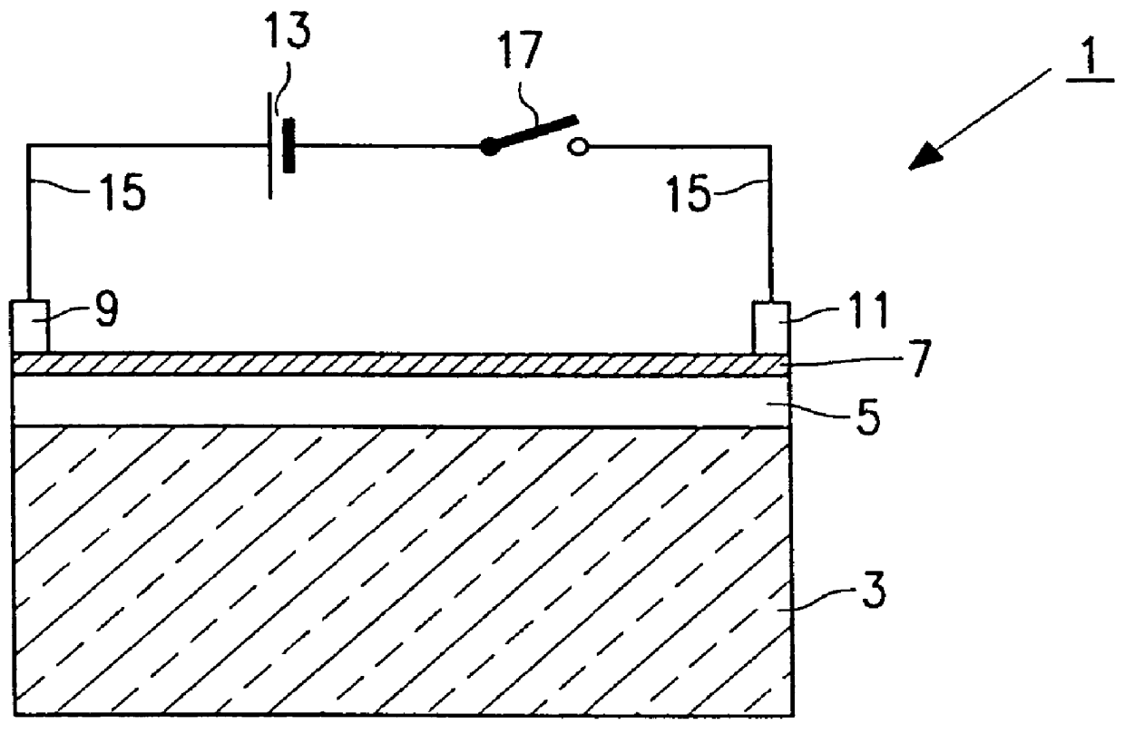
FIG. 1 is a schematic, cross-sectional view of a switching device 1 in accordance with the invention. In this FIGURE, the layer thicknesses are not drawn to scale. A glass substrate 3, having a thickness of 0.5 mm, is provided with a 300 nm thick yttrium film, which serves as a switching film 5, by means of electron-beam evaporation. The residual pressure in the evaporation apparatus is less than 10.sup.-7 mbar. The deposition rate is 0.5 nm / s. In the same apparatus, a 30 nm thick capping layer 7 of palladium is evaporated onto the switching film 5 by means of resistance heating. The capping layer 7 is provided with copper terminals 9 and 11 by soldering.

The switching film 5 is subsequently exposed to molecular hydrogen via the capping layer 7, at a pressure of 1.5 bar (1.5.times.10.sup.5 Pa) and at room temperature in an enclosure (not shown) which is shut off from the environment. The capping layer 7 forms atomic H, which is subsequently absorbed in the switching film 5. After 5 s...


PUM

PropertyMeasurementUnit
thicknessaaaaaaaaaa
thicknessaaaaaaaaaa
temperatureaaaaaaaaaa

Abstract

A description is given of an optical switching device (1) comprising a transparent substrate (3), a switching film (5) of a hydride compound of a trivalent transition or rare earth metal having a thickness of 300 nm, and a palladium capping layer (7) having a thickness of 30 nm. The capping layer is in contact with hydrogen. An electric current through the switching film (5) can be switched on and off between the terminals (9, 11). Joule heating of the switching film (5) causes a rapid transition from the transparent trihydride state to the absorbing dihydride state. By switching off the current, the switching film (5) cools down, which results in the formation of the absorbing dihydride state. The conversion between both states is reversible and can be repeated many times. The device can be used for controlling light beams, or it can be used in or for a display. Optionally, cooling of the switching film (5) is obtained with a Peltier element in thermal contact with the switching film (5).

Description

The invention relates to an optical switching device comprising:a substrate,a switching film formed on the substrate, which switching film comprises a hydride of a trivalent transition or rare earth metal and can be reversibly switched from a light-absorbing dihydride state to a transparent trihydride state by an exchange of hydrogen,a capping layer formed on the switching film, the capping layer being capable of hydrogen dissociation, anda hydrogen source which is in contact with the capping layer.The invention also relates to the use of such a switching device.In optical switching devices, the optical properties are governed by external influences, such as gas pressure, an electric voltage or current, temperature or light.For example, electrochromic devices are well-known in which a layer of an electrochromic material, such as MoO.sub.3, is sandwiched between two transparent electroconductive electrode layers, for example, of indium-tin oxide. A layer of an H.sup.+ - or Li.sup.+ -...

Claims


Application Information

Patent Timeline
Patent Type & Authority Patents(United States)
IPC IPC(8): G02F1/01G02F1/15G02F1/17G02F3/02H03K17/78
CPCG02F1/1523G02F1/17G02F1/0147G02F2202/34
Inventor DEN BROEDER, FRIEDRICH J. A.HANZEN, RALPH M. N.DUINE, PETER A.JUNGBLUT, REINER M.DRAIJER, CORNELISROOZEBOOM, FREDDYVAN DER SLUIS, PAUL
Owner U S PHILIPS CORP
Why Eureka
Try Eureka