

Digital wave shaping circuit, frequency multiplying circuit, and external synchronizing method, and external synchronizing circuit
a digital wave and frequency multiplying technology, applied in the field of digital wave shaping circuits, frequency multiplying circuits, external synchronizing methods and external synchronizing circuits, can solve the problems of loss of phase division meaning, disadvantageous economic aspects and in view of heating the elements, and destruction of signal wave forms
- Summary
- Abstract
- Description
- Claims
- Application Information
AI Technical Summary
Problems solved by technology
Method used
Image

Examples
Embodiment Construction
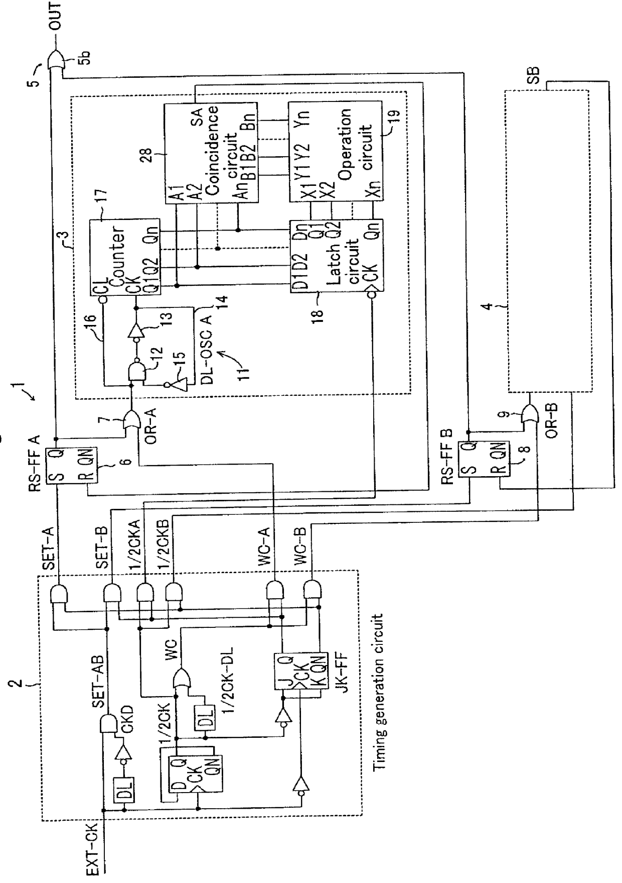
A1though a presettable D-FF 54 is used for a width forming circuit 5 in the above-mentioned preferred embodiments, as shown in FIG. 20, it is possible to secure a required output ((33) IN FIG. 18) by taking out an Q output of RS-FF 6, 8 positioned before each of the above-mentioned duty determination circuits 3A, 4A, 3B, 4B by the OR gate 56 with the output OR gate 56 employed instead of D-FF 54.
A1though a description of the operations of this preferred embodiment is omitted, the embodiment is such that the outputs Q of the prepositioned flip flops 6, 8, that is, RS-FF-A1-Q (P3, P4, P11, P12), RS-FF-A2-Q (P1, P2, P9, P10), RS-FF-B1-Q (P7, P8), RS-FF-B2-Q (P5, P6) in FIG. 17 and FIG. 18 are merely synthesized and is characterized in that the Q output of these prepositioned flip flops 6,8 are taken out as outputs. An advantage of such a construction is in that the circuit configuration is further simplified than that shown in FIG. 10.
Furthermore, although in the above preferred embodi...
PUM
 Abstract
Description
Claims
Application Information