Liquid crystal display device with arrangement of common electrode portion and image signal electrode

a liquid crystal display device and electrode electrode technology, applied in non-linear optics, instruments, optics, etc., can solve the problems of preventing the precise manufacture of active devices, point or line defects, and high cost of manufacturing such standard liquid crystal display devices, and achieves high aperture factor, reduce aperture factors, and suffix aperture factors

Inactive Publication Date: 2000-09-26
PANASONIC LIQUID CRYSTAL DISPLAY CO LTD +1
View PDF6 Cites 40 Cited by
  • Summary
  • Abstract
  • Description
  • Claims
  • Application Information

AI Technical Summary

Benefits of technology

The present invention permits a sufficient aperture factor to be maintained, without losing the described advantages (1) and (2) discussed above. Instead of structures such as comb shaped electrodes which inevitably reduce the aperture factor, the more simple structure of the electrode permits a practical high aperture factor to be achieved.
The first aspect of the invention discussed above relates to structures in which the common electrodes are formed on the mutually facing interfaces of substrates, or the pixel electrodes are formed on a same layer. In (JP-B-63-21907 (1988)), the directions of the signal wiring and the common electrode cross over at the right angles to each other in order to form the comb shaped electrodes. That is, the signal wiring extends in a first direction (Y direction), and the common electrode extends in a direction perpendicular to the first direction (X direction). On the other hand, the present invention permits the avoidance of a complex structure such as comb shaped electrodes by having the signal wiring, the pixel electrode, and the common electrode all extending in a common direction. In order to reduce the threshold voltage of the liquid crystal and to shorten the response time, it is preferable to make the interval between the pixel electrode and the common electrode narrow, locating the pixel electrode and the signal wiring electrode between a pair of common electrodes is also effective and it is not necessary to use a complex structure such as a comb shaped electrode.
The second aspect of the present invention also permits the structure to be simplified and the aperture factor increased by providing the pixel electrode and the common electrode in different layers separated from each other by an insulating layer. This aspect of the present invention differs substantially from JP-B-63-21907 (1988) in that the pixel electrode and the common electrode are provided in separated layers. One advantage of this is that the region for the additional capacitive device which has been reduced by use of the lateral electric field system can be further reduced. Thus, overlapping of the pixel electrode and the common electrode separated by an insulating film becomes possible because they are in separate layers, and a load capacitance can be formed in the region of overlap. The overlapping parts can be used as a part of the wiring for the common electrodes. Hence, it is not necessary to sacrifice a part of the display in order to form a capacitive device. Accordingly, the aperture factor for the pixel can be further increased.
Depending on a design of each pixel, a plurality of capacitive devices can be formed. Hence, the voltage holding characteristics may be significantly improved, and deterioration of the display quality rarely occurs even if severe contamination of the liquid crystal and lowering of off-resistance of the thin film transistor are generated. Furthermore, the insulating film formed between the pixel electrode and the common electrode can be commonly used in common as a gate insulating film of the scanning wiring (gate line) in the same layer. Therefore, there is no need to form a further film, and a process step for providing separate layers is not necessary.
There are other advantages of the separate layers formed by insertion of the insulating film between the pixel electrode and the common electrode for example the probability of short-circuit failures between the pixel and common electrodes can be reduced significantly due to the existence of the insulating film therebetween, and accordingly, the probability of pixel defects can be reduced.

Problems solved by technology

However in order to form such transparent electrodes, it is necessary to use a vacuum manufacturing operation, such as sputtering, and thus the cost of manufacture of such standard liquid crystal display devices is high.
Furthermore, it has been found that such transparent electrodes have vertical geometrical irregularities, of the order of several tens of nanameters, this prevent precise manufacture of active devices, such as thin film transistors needed to control the signals to the electrodes.
Also, it has been found that parts of such transparent electrodes may come detached, to cause point or line defects.
Thus, it has proved difficult to manufacture both reliably and cheaply liquid crystal devices.
Such conventional liquid crystal display devices also have disadvantages in terms of picture quality.
The problem of vertical geometrical irregularities in the transparent electrodes has been mentioned above, but similar irregularities around the controlling transistors may result in orientation failure domains being formed, requiring light shielding film to cover such transistor devices, using the light utilisation efficiency of the liquid crystal device.
Also, such conventional liquid crystal display devices have disadvantage that their significant change in brightness when the visual angle is changed, and reversion of some gradation levels can occur in a half-term display, at some view angles.
Although the use of comb shaped electrodes, such as previously discussed, prove the need for transparent electrodes, further problems have been found.
While the use of such comb-shaped electrodes offers theoretical advantages, those are limited by practical consideration which have to be taken into account when the comb-shaped electrodes are used.
However, It is extremely difficult to form such fine teeth over a large substrate without defects.
There is thus a trade-off between aperture factor and production yield, which is undesirable.

Method used


Image

  • Liquid crystal display device with arrangement of common electrode portion and image signal electrode
  • Liquid crystal display device with arrangement of common electrode portion and image signal electrode
  • Liquid crystal display device with arrangement of common electrode portion and image signal electrode

Examples


embodiment 2

In the second embodiment, the scanning electrode which had been arranged on the substrate facing the substrate supporting the pixel in the first embodiment was formed on the same substrate as the pixel electrode. The rest of the structure of the second embodiment is generally the same as that of the first embodiment and corresponding parts are indicated by the same reference numerals. The cross section of the structure of the thin film transistor and the electrodes in the second embodiment are shown in FIG. 4. The pixel electrode 1, the signal electrode 12, and the scanning electrode 10 were all made from aluminum, and were formed simultaneously by deposited and etched. There is no conductive material on the other substrate. Hence, in this structure, even if the conductive material is contaminated during the manufacturing process, there is no possibility of upper and lower electrodes touching each other, and defects due to the upper and lower electrodes touching is eliminated. There...

embodiment 3

The structure of the third embodiment is generally the same as the first embodiment 1 except as will be described below. Components which correspond to components of the first embodiment are indicated by the same reference numerals.

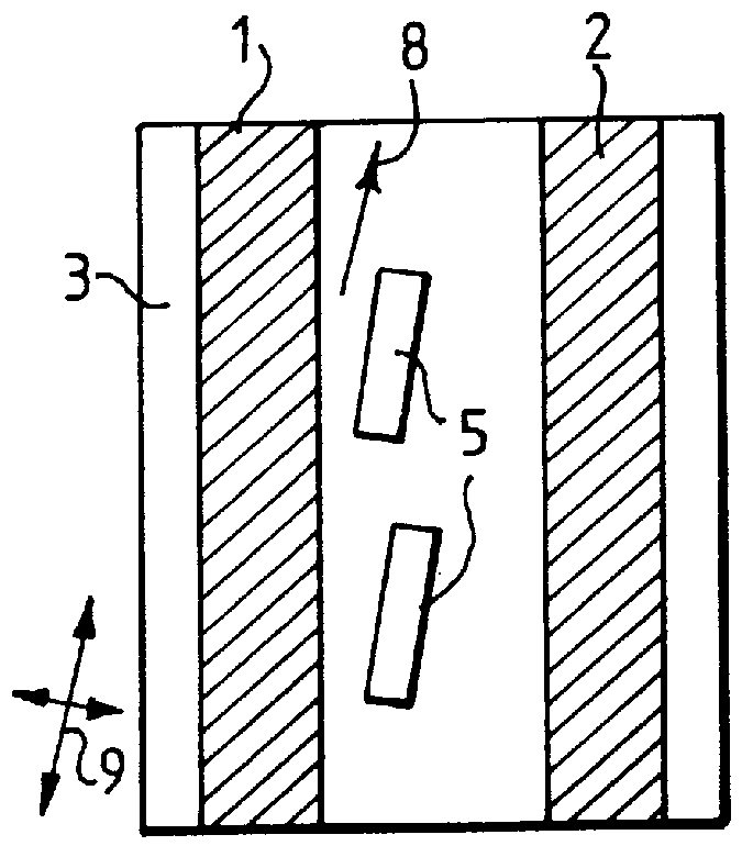
The structure of the thin film transistor and the various electrodes of the third embodiment is shown in FIGS. 5(a) and 5(b). The signal electrode 12 was arranged between a pair of pixel electrodes 1 and a pair of common electrodes 2 were arranged outside the above electrodes. A signal wave having information is applied to the signal electrode 12, and a scanning wave is applied to the scanning electrode 10 synchronously with the signal wave. A thin film transistor comprising amorphous silicon (a--Si) 16 and an insulating-protecting film 15 of silicon nitride (SiN) is arranged substantially centrally between a pair of common electrodes. The same information signals are transmitted from the signal electrode 12 to each of two pixel electrodes 1 through two t...

embodiment 4

The structure of the fourth embodiment is generally the same as the first embodiment except as will be described below. Components of the fourth embodiment which correspond to the first embodiment are indicated by the same reference numerals.

FIG. 15(a) is a partial plan view of an active matrix type liquid crystal display device being the fourth embodiment. FIG. 15(b) is a cross sectional view taken on line A-A' in FIG. 15(a), and FIG. 15(c) is a cross sectional view taken on line B-B' in FIG. 15(a). The capacitive device 11 which had a structure in which the gate insulating film composed from silicon nitride 13 was located between the pixel electrode 1 and the scanning wiring 10 in the first embodiment 1 was changed to a structure in which the liquid crystal composition layer 50 extended between parts of the pixel electrode 1 and the common electrode 2 which faced each other, as shown in FIG. 15(c).


PUM

PropertyMeasurementUnit
widthaaaaaaaaaa
thicknessaaaaaaaaaa
thicknessaaaaaaaaaa

Abstract

A liquid crystal display device has a plurality of pixel elements, the optical transmissivity of which is varied by suitable electrical signals. The liquid crystal display device has electrodes which apply electric fields to a liquid crystal layer, the electric fields having components in a direction generally parallel to the liquid crystal layer. Each pixel element has at least one pixel electrode which extends in a common direction as a signal electrode and common electrodes which extend over several pixel elements. The common electrodes may be on the same side of the liquid crystal layer as the pixel and signal electrodes, or they may be on opposite sides. Each pixel may have two pixel electrodes with the signal electrode disposed therebetween, and there are then a pair of common electrodes with the pixel electrodes therebetween. The common electrodes may be common to adjacent pixel elements. The pixel electrodes and the common electrodes may be separated by an insulating film.

Description

1. Field of the InventionThe present invention relates to a liquid crystal display device having at least one, preferably a plurality, of pixel elements.2. Description of the Prior ArtIn standard liquid crystal display device, the pixel element is a liquid crystal layer (normally common to the pixel elements) extending in a plane, and there is at least one polarizing means parallel to the plane of the liquid crystal layer. By applying electrical signals to the liquid crystal layer using suitable electrodes, it is possible to vary the angle of polarization of polarized light passing through the liquid crystal layer. Thus, by changing those electrical signals, it is possible to vary the optical transmissivity of a liquid crystal display device by varying the change in polarization relative to the at least one polarizing means. Normally, in such a liquid crystal display device, the polarizing means is formed by two polarizing plates, one on each side of the liquid crystal layer, but is...

Claims


Application Information

Patent Timeline
Patent Type & Authority Patents(United States)
IPC IPC(8): G02F1/13G02F1/1343G02F1/1362G02F1/1368
CPCG02F1/134363G02F1/136213G02F1/1368G02F2201/122G02F2201/128G02F1/1343
Inventor KONDO, KATSUMITERAO, HIROMUABE, HIDETOSHIOHTA, MASUYUKISUZUKI, KENKICHISASAKI, TOHRUKAWACHI, GENSHIROOHWADA, JUNICHI
Owner PANASONIC LIQUID CRYSTAL DISPLAY CO LTD
Why Eureka
Try Eureka