Liquid crystal display device with common electrode arrangement
a liquid crystal display device and electrode arrangement technology, applied in non-linear optics, instruments, optics, etc., can solve the problems of preventing the precise manufacture of active devices, point or line defects, and high cost of such standard liquid crystal display devices, and achieves reduced aperture factors, simple structure, and sufficient aperture factor
- Summary
- Abstract
- Description
- Claims
- Application Information
AI Technical Summary
Benefits of technology
Problems solved by technology
Method used
Image
Examples
first embodiment
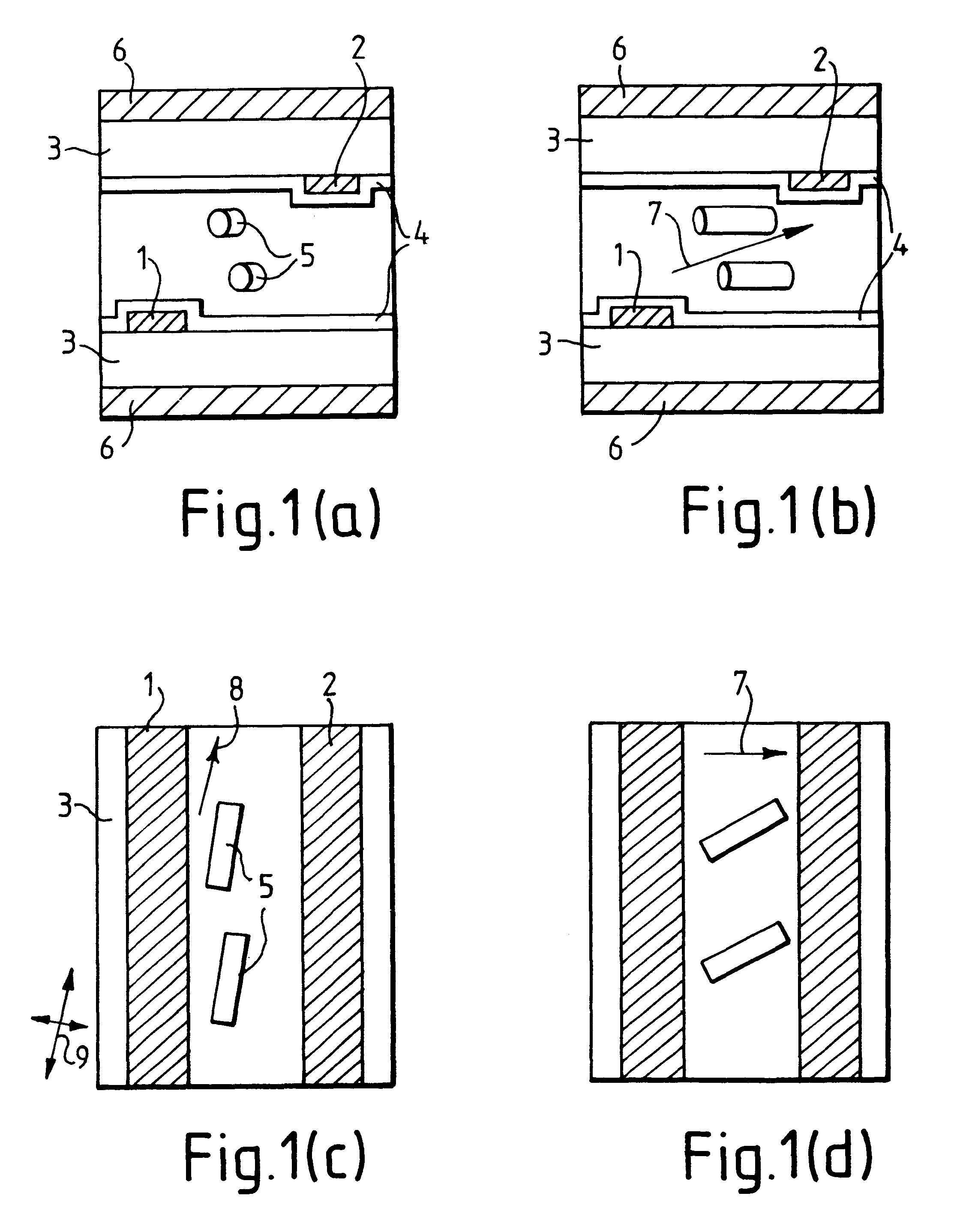
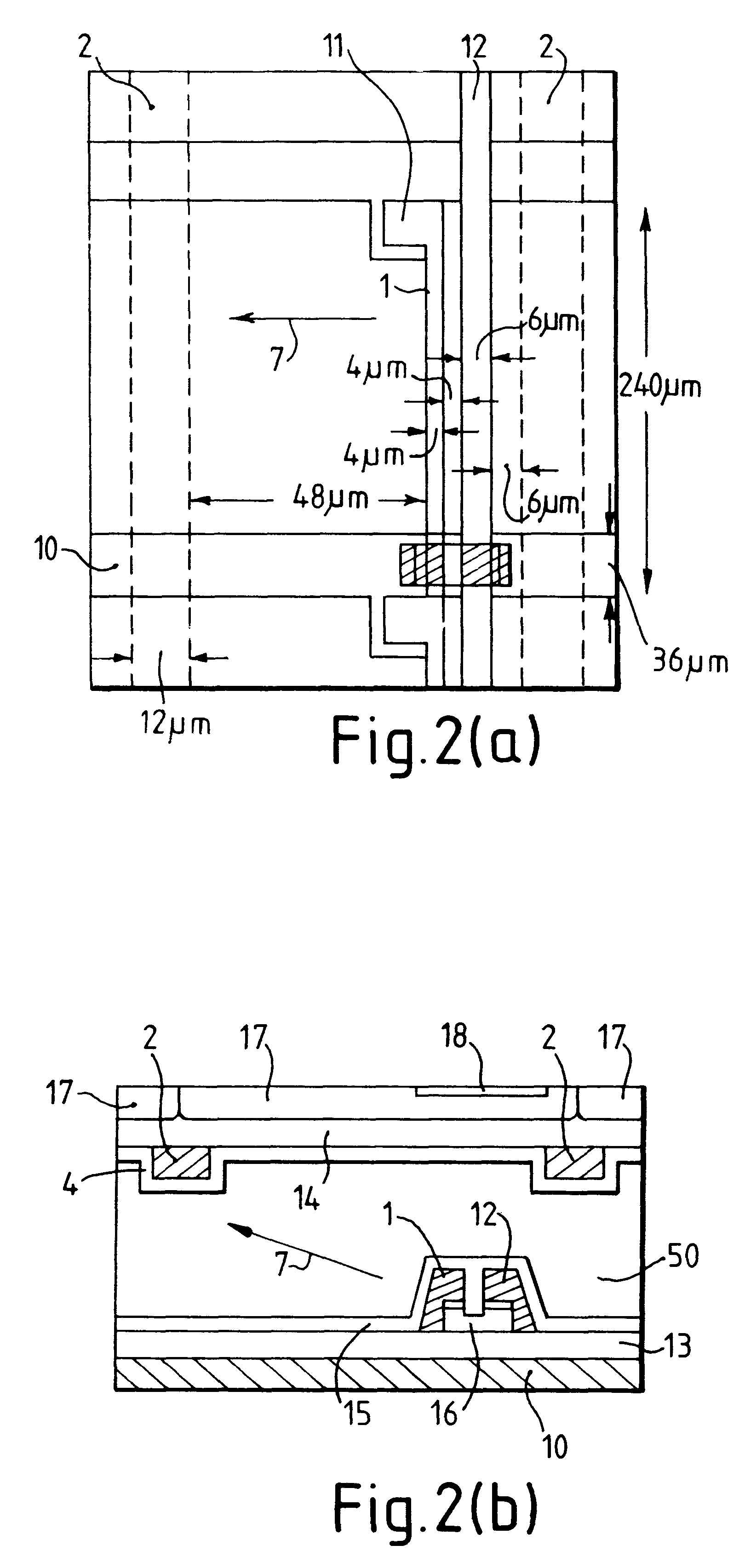
In the first embodiment shown in FIGS. 2(a) and 2(b), two glass substrates (not shown in FIG. 2(a) or 2(b) but as shown in FIGS. 1(a) to 1(d)) were used which were polished on the surfaces and 1.1 mm thick. Between these substrates was interposed a nematic liquid crystal which had a positive dielectric constant anisotropy .DELTA..di-elect cons. of 4.5 and a birefringence .DELTA.n of 0.072 (589 nm, 20 C.degree.). A polyimide orientation control film applied over the substrate surface was subjected to a rubbing processing to produce a pretilt angle of 3.5 degrees. The rubbing directions of the upper and the lower interfaces were almost parallel and at an angle of 85 degrees (.phi..sub.LC1 =.phi..sub.LC2 =85.degree.) with respect to the direction of the applied electric field.
A gap d was formed by dispersing spherical polymer beads between the substrates so that the gap became 4.5 .mu.m when the liquid crystal was sealed. Hence, .DELTA.n.multidot.d was 0.324 .mu.m. The resulting struct...
embodiment 2
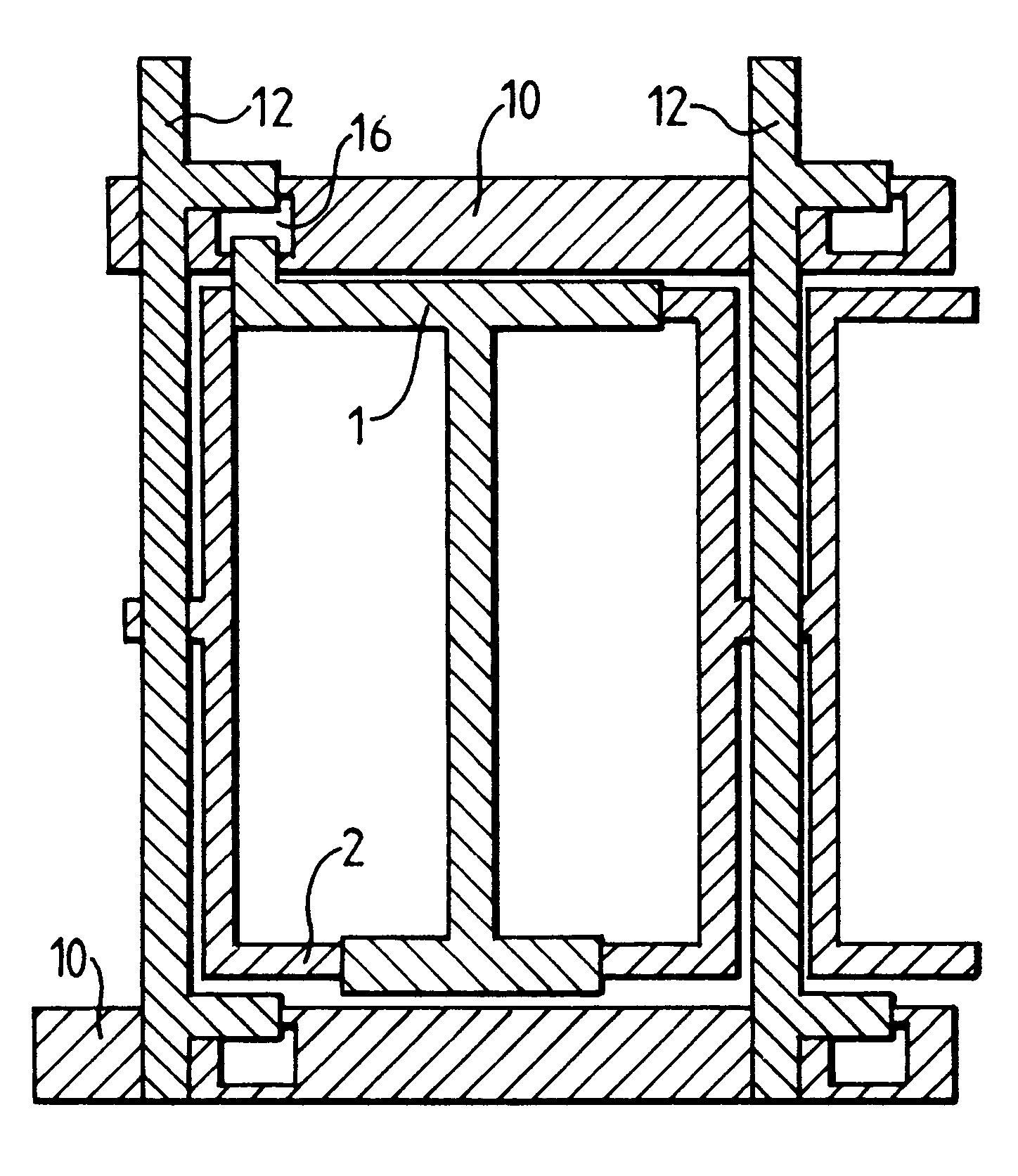
In the second embodiment, the scanning electrode which had been arranged on the substrate facing the substrate supporting the pixel in the first embodiment was formed on the same substrate as the pixel electrode. The rest of the structure of the second embodiment is generally the same as that of the first embodiment and corresponding parts are indicated by the same reference numerals. The cross section of the structure of the thin film transistor and the electrodes in the second embodiment are shown in FIG. 4. The pixel electrode 1, the signal electrode 12 and the scanning electrode 10 were all made from aluminum, and were formed simultaneously by being deposited and etched. There is no conductive material on the other substrate. Hence, in this structure, even if the conductive material is contaminated during the manufacturing process, there is no possibility of upper and lower electrodes touching each other, and so defects due to the upper and lower electrodes touching is eliminate...
second embodiment
Generally, the precision of alignment of photomasks is significantly higher than that for two facing glass substrates. Therefore, variations in the alignment of the electrodes can be suppressed when all of the four electrodes are formed on only one of the substrates, as in the second embodiment, because alignment of the electrodes during manufacturing can be only applied to photomasks. Therefore, the present embodiment is suitable for forming more precise patterns in comparison with the case when the scanning electrode is formed on the other substrate.
A bright display having the same wide visual angle as the first embodiment was obtained.
PUM
| Property | Measurement | Unit |
|---|---|---|
| width | aaaaa | aaaaa |
| thickness | aaaaa | aaaaa |
| thickness | aaaaa | aaaaa |
Abstract
Description
Claims
Application Information


