

Connector for a printed circuit board and a production method therefor
- Summary
- Abstract
- Description
- Claims
- Application Information
AI Technical Summary
Benefits of technology
Problems solved by technology
Method used
Image

Examples
Embodiment Construction
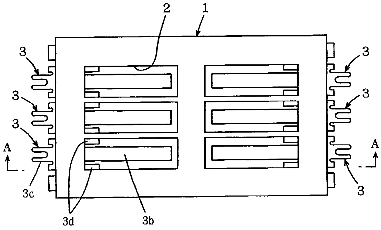
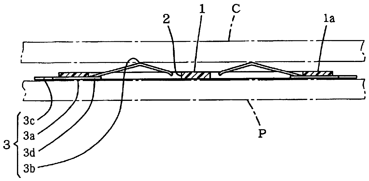
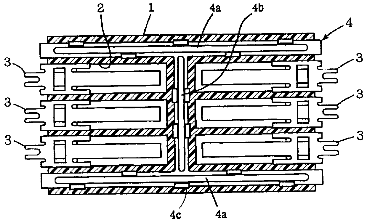
In the following, some embodiments of the present invention will be described with reference to drawings. FIG. 1 through FIG. 4 show a connector for a printed circuit board according to the first embodiment. This connector connects a printed circuit board P built in a portable telephone and an SIM card C of GSM standard that stores, for example, personal data. It is a board to card connector.
In these diagrams, 1 denotes a board-shaped housing made of an insulating material, for example, a heat resistant resin or the like. This housing is provided with a total of six windows 2, two rows.times.three columns. In each window 2, a connecting terminal 3 is provided. The connecting terminal is made of, for example, a copper alloy, and is given gold plating, etc. when necessary. This connecting terminal 3 has an intermediate part 3a that is fixed to a housing part 1a at the edge of the window. The internal end of the connecting terminal 3 is bent into an inverted V shape in the window 2 to ...
PUM
 Abstract
Description
Claims
Application Information