Memory device with address translation for skipping failed memory blocks

a memory device and address translation technology, applied in the field of semiconductor memory devices, can solve problems such as memory cell defects, semiconductor memory devices that cannot function properly, and semiconductor memory devices considered defectiv

Inactive Publication Date: 2001-02-13
SAMSUNG ELECTRONICS CO LTD
View PDF4 Cites 35 Cited by
  • Summary
  • Abstract
  • Description
  • Claims
  • Application Information

AI Technical Summary

Problems solved by technology

However, during manufacture of the memory device, some of the memory cells may be defective.
However, if the number of failed memory cells is greater than the number of redundant memory cells capable of replacing the failed memory cells, the semiconductor memory device will not function properly.
Thus, if any failed memory cells remain after the repair process, the semiconductor memory device is considered to be defective.

Method used


Image

  • Memory device with address translation for skipping failed memory blocks
  • Memory device with address translation for skipping failed memory blocks
  • Memory device with address translation for skipping failed memory blocks

Examples


Embodiment Construction

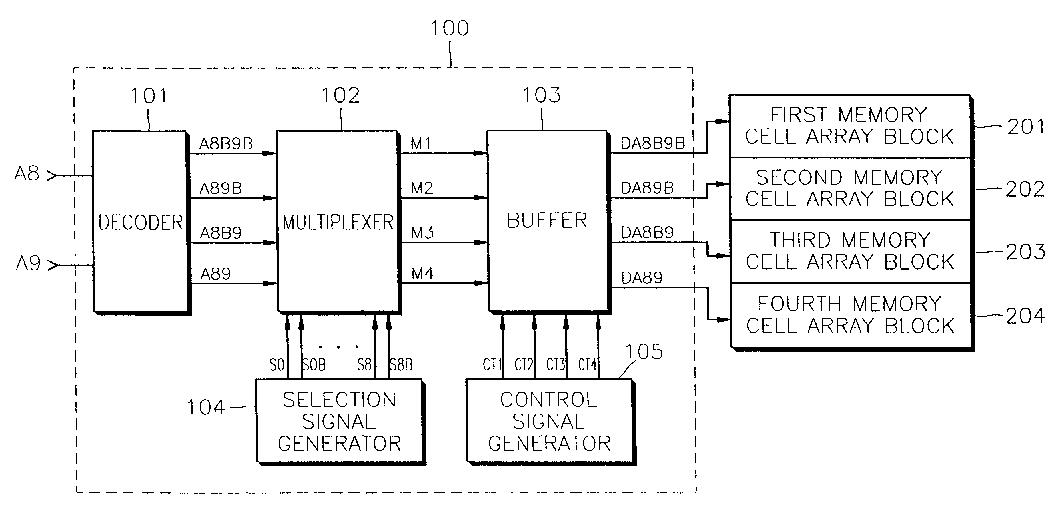
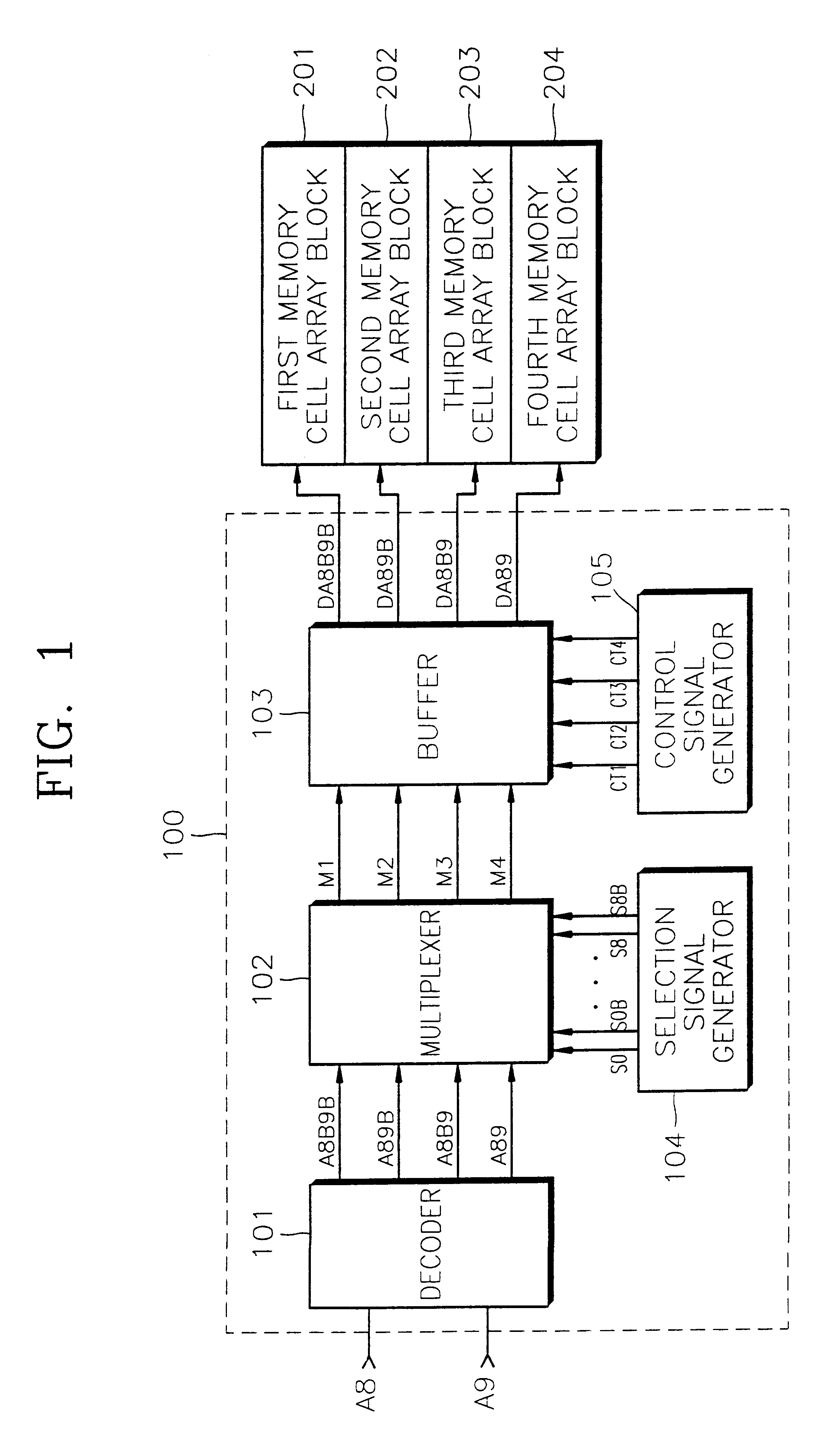
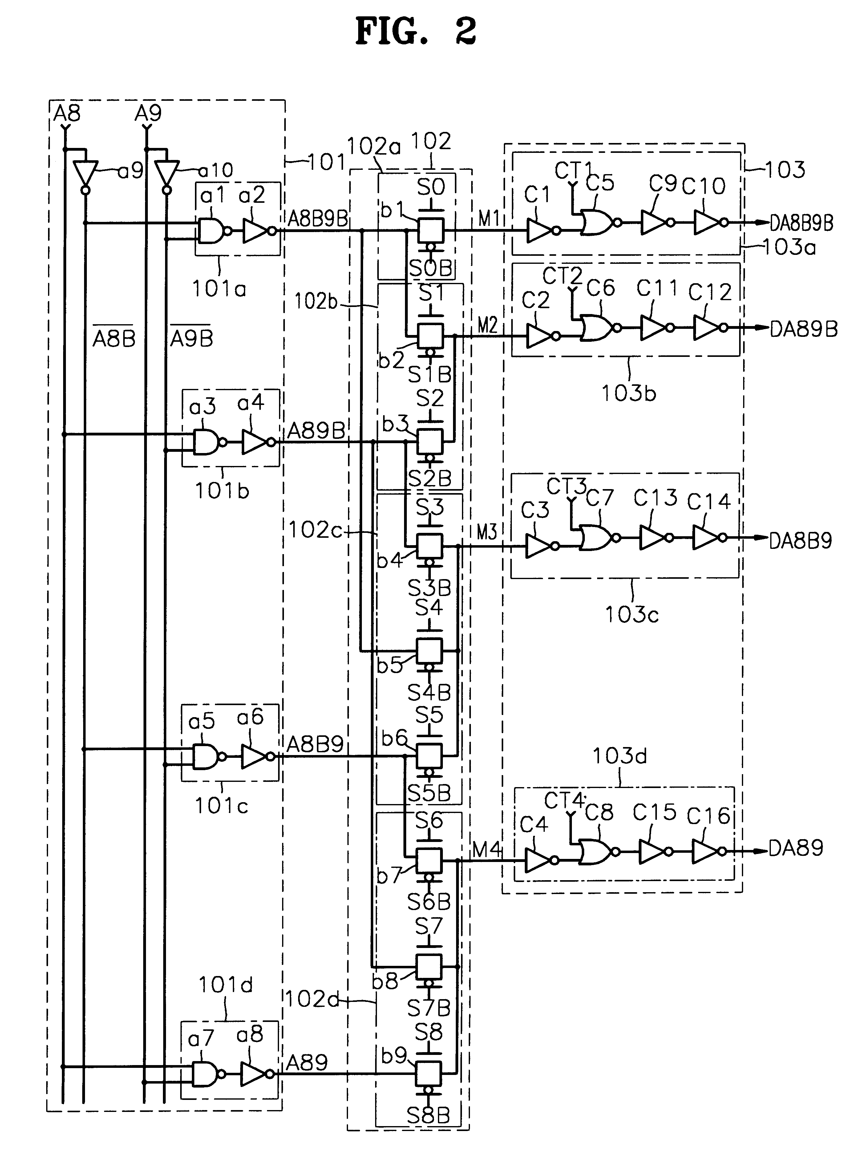
Referring to FIG. 1, a semiconductor memory device according to the present invention includes first through fourth memory cell array blocks 201-204, and address decoding circuitry 100 for receiving an address (A8, A9). The address decoding circuitry 100 accesses only memory cell array blocks having normally operating memory cells ("good memory cell array blocks") among the first through fourth memory cell array blocks 201-204. The address decoding circuitry 100 skips over any memory cell array block which includes one or more failed memory cells which have not been replaced by redundant memory cells during the repair process ("failed memory cell array blocks"). Only four memory cell array blocks are shown in FIG. 1 for ease of explanation. However, it is obvious that more memory cell array blocks can be included. The address decoding circuitry of the present invention can be adapted for use with semiconductor memory devices having a large number of memory cell array blocks, as will...


PUM


Abstract

A semiconductor memory device capable of operating normally even when a failed memory cell remains after repair. The semiconductor memory device includes a plurality of memory cell array blocks, and address decoding circuitry for receiving an address and for accessing good memory cell array blocks and skipping failed memory cell array blocks.

Description

1. Field of the InventionThe present invention relates generally to a semiconductor device, and more particularly, to a semiconductor memory device capable of operating normally even when a failed memory cell exists after repair.2. Description of the Related ArtA semiconductor memory device includes a plurality of memory cells which must be function properly in order for the memory device to function properly. However, during manufacture of the memory device, some of the memory cells may be defective. To solve this problem, semiconductor memory devices include redundant memory cells capable of being used in place of such failed memory cells. When failed memory cells are detected, the failed memory cells are replaced by the redundant memory cells to "repair" the memory device. This procedure improves the manufacturing yield, reducing the cost of manufacture of the memory devices.However, if the number of failed memory cells is greater than the number of redundant memory cells capable...

Claims


Application Information

Patent Timeline
Patent Type & Authority Patents(United States)
IPC IPC(8): G11C8/12G11C8/00G11C29/00
CPCG11C8/12G11C29/76G11C29/88G11C29/883G11C29/00
Inventor JUNG, SEONG-OOK
Owner SAMSUNG ELECTRONICS CO LTD
Why Eureka
Try Eureka