Printed circuit board with capacitors connected between ground layer and power layer patterns

a printed circuit board and capacitor technology, applied in the direction of line-transmission details, sustainable manufacturing/processing, final product manufacturing, etc., can solve the problems of device malfunction, reduced mounting density, and inability of cage structure to suppress electromagnetic waves from radiating,

Inactive Publication Date: 2001-03-06
NEC CORP
View PDF10 Cites 164 Cited by
  • Summary
  • Abstract
  • Description
  • Claims
  • Application Information

AI Technical Summary

Problems solved by technology

In advanced information society, undesired electromagnetic waves radiated from electronic devices such as information processing devices and communicating devices disturb broadcasting and radio communication systems and cause devices to malfunction.
In this case, the cage structure cannot suppress an electromagnetic wave from radiating.
In the IC card 111 shown in FIG. 21 and the liquid crystal displaying device shown in FIG. 22, since the printed circuit board requi

Method used


Image

  • Printed circuit board with capacitors connected between ground layer and power layer patterns
  • Printed circuit board with capacitors connected between ground layer and power layer patterns
  • Printed circuit board with capacitors connected between ground layer and power layer patterns

Examples


first embodiment

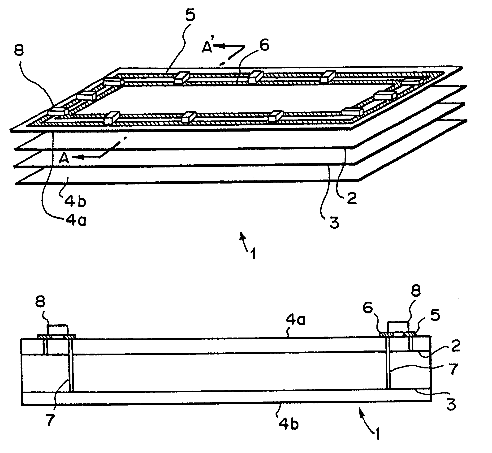
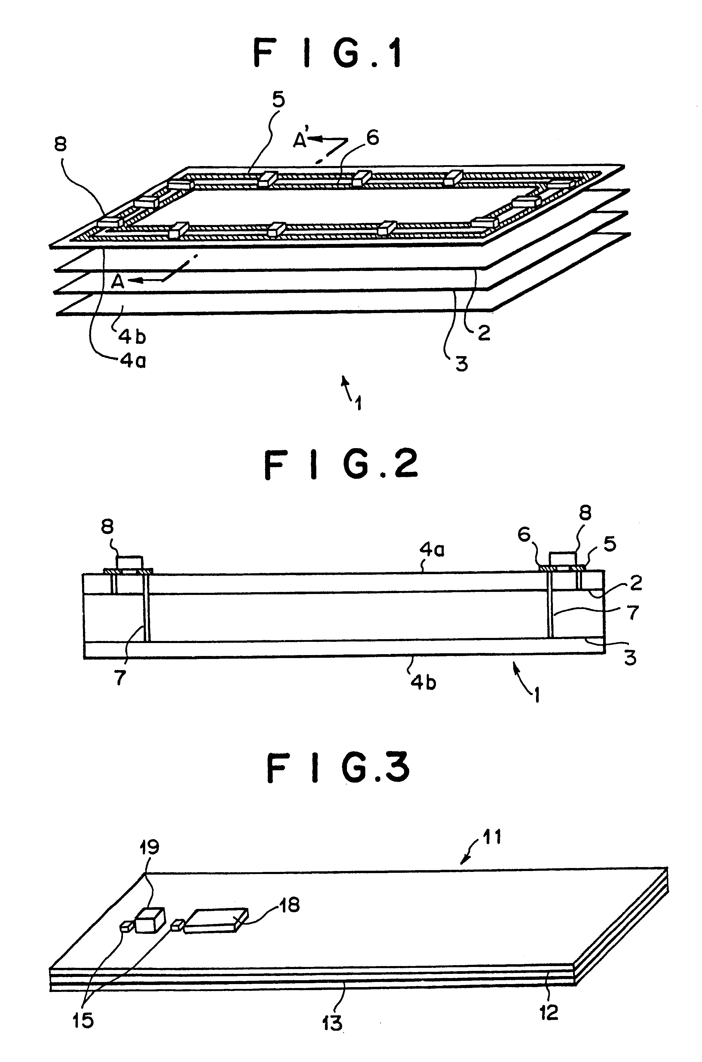
Next, with reference to the accompanying drawings, embodiments of the present invention will be described. FIGS. 1 and 2 show the structure of a laminated printed circuit board 1 according to the present invention. FIG. 1 is an exploded perspective view showing the structure of individual layers of the printed circuit board 1. FIG. 2 is a sectional view taken along the line A-A' shown in FIG. 1.

The printed circuit board 1 has four metal layers on which circuit patterns are formed by electrolytic plating method. Each layer is separated with an insulator (not shown) composed of such as glass epoxy or paper phenol. The four layers of the printed circuit board 1 are referred to as a first layer, a second layer, a third layer, and a fourth layer that are successively disposed from the top thereof. The first layer and the fourth layer are used as signal wiring layers 4a and 4b for wiring signal lines. The second layer is a ground layer 2. The third layer is a power supply layer 3. So-call...

second embodiment

FIGS. 7 and 8 show the structure of a laminated printed circuit board 21 according to the present invention. FIG. 7 is an exploded perspective view showing the printed circuit board 21. FIG. 8 is a sectional view taken along line A A' shown in FIG. 7.

The printed circuit board 21 has four metal layers on which circuit patterns are formed by electrolytic plating method. Each layer is separated with an insulator composed of such as glass epoxy or paper phenol. The four layers of the printed circuit board 21 are referred to as a first layer, a second layer, a third layer, and a fourth layer that are successively disposed from the top thereof. The first layer and the fourth layer are used as signal wiring layers 24 for wiring signal lines. The second layer is a ground layer 22. The third layer is a power supply layer 23. So-called solid patterns are formed on the entire surfaces of the ground layer 22 and the power supply layer 23.

On the periphery of the printed circuit board, a top laye...

third embodiment

FIGS. 10 and 11 show the structure of a laminated printed circuit board 31 according to the present invention. FIG. 10 is an exploded perspective view of the printed circuit board 31. FIG. 11 is a sectional view taken along line A A' shown in FIG. 10.

The printed circuit board 31 has four metal layers on which circuit patterns are formed by electrolytic plating method. Each layer is separated with an insulator composed of such as glass epoxy or paper phenol. The four layers of the printed circuit board 31 are referred to as a first layer, a second layer, a third layer, and a fourth layer that are successively disposed from the top thereof. The first layer and the fourth layer are used as signal wiring layers 34 for wiring signal lines. The second layer is a ground layer 32. The third layer is a power supply layer 33. So-called solid patterns are formed on the entire surfaces of the ground layer 32 and the power supply layer 33.

On the first layer 34a as the top layer, a plurality of c...


PUM


Abstract

A printed circuit board is disclosed. A top layer power supply pattern and a top layer ground pattern are formed. The top layer power supply pattern and the top layer ground pattern are connected to a power supply layer and a ground layer through a plurality of viaholes, respectively. A plurality of capacitors or a plurality of capacitor resistor series circuits are disposed at predetermined intervals between the top layer power supply pattern and the top layer ground pattern.

Description

1. Field of the InventionThe present invention relates to a laminated printed circuit board that has at least two layers and that are used for electronic devices such as information processing devices and communicating devices, in particular, to a laminated printed circuit board having a function for suppressing an undesired electromagnetic wave from radiating.2. Description of the Related ArtIn advanced information society, undesired electromagnetic waves radiated from electronic devices such as information processing devices and communicating devices disturb broadcasting and radio communication systems and cause devices to malfunction. To suppress undesired electromagnetic waves from radiating and prevent them from entering such devices, shields and filters are used.As a method for suppressing an undesired electromagnetic wave radiated from an electronic device, an electromagnetic wave radiated from a printed circuit board as a radiation source is enclosed with a shield. Alternati...

Claims


Application Information

Patent Timeline
IPC IPC(8): H05K1/02H05K1/11H05K9/00H05K3/46
CPCH05K1/0231H05K1/0234H05K1/112H05K2201/09309H05K2201/09345H05K2201/09354H05K2201/0979H05K2201/10022H05K2201/10446H05K2201/10636H01L2224/16225H01L2924/19105Y02P70/50
Inventor HARADA, TAKASHISASAKI, HIDEKI
Owner NEC CORP
Why Eureka
Try Eureka