Methods for errors checking the configuration SRAM and user assignable SRAM data in a field programmable gate array

a technology of sram and configuration sram, applied in the field of field programmable gate array (fpga) integrated circuits, can solve problems such as event upset, data in configuration sram is susceptible to at least one bit change, and is not considered acceptable, and the undetected occurrence of a seu is not considered acceptabl

Inactive Publication Date: 2001-05-22
MICROSEMI SOC
View PDF7 Cites 90 Cited by
  • Summary
  • Abstract
  • Description
  • Claims
  • Application Information

AI Technical Summary

Problems solved by technology

Hence, one of the primary disadvantages in using configuration SRAM is that the data in the configuration SRAM is susceptible to an unintended change of at least one bit, known as single event upset (SEU).
In certain high reliability applications the undetected occurrence of a SEU is not considered acceptable.
The reluctance among design engineers to use SRAM configured FPGA's in high reliability applications such as space, aeronautics, and military equipment due to the vulnerability to SEU's in harsh environments is well known.
Though lowering the probability of an SEU in a harsh environment may be accomplished, eliminating the possibility of an SEU altogether seems unlikely.
However, providing this memory by having other than explicitly dedicated SRAM blocks included in the FPGA has not proved satisfactory.
When user-assignable SRAM is implemented with the logic modules in the FPGA, it requires a substantial amount of the routing and lo

Method used


Image

  • Methods for errors checking the configuration SRAM and user assignable SRAM data in a field programmable gate array
  • Methods for errors checking the configuration SRAM and user assignable SRAM data in a field programmable gate array
  • Methods for errors checking the configuration SRAM and user assignable SRAM data in a field programmable gate array

Examples


Embodiment Construction

Those of ordinary skill in the art will realize that the following description of the present invention is illustrative only and not in any way limiting. Other embodiments of the invention will readily suggest themselves to such skilled persons.

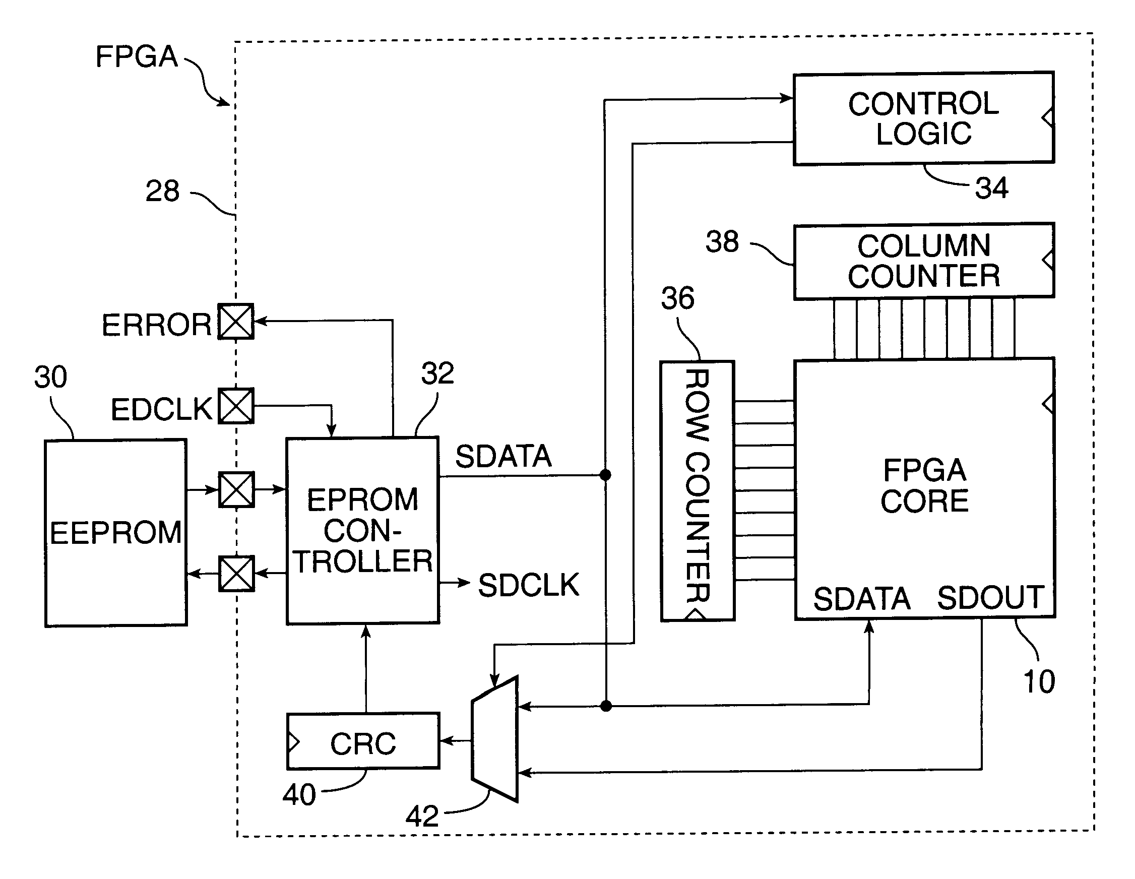
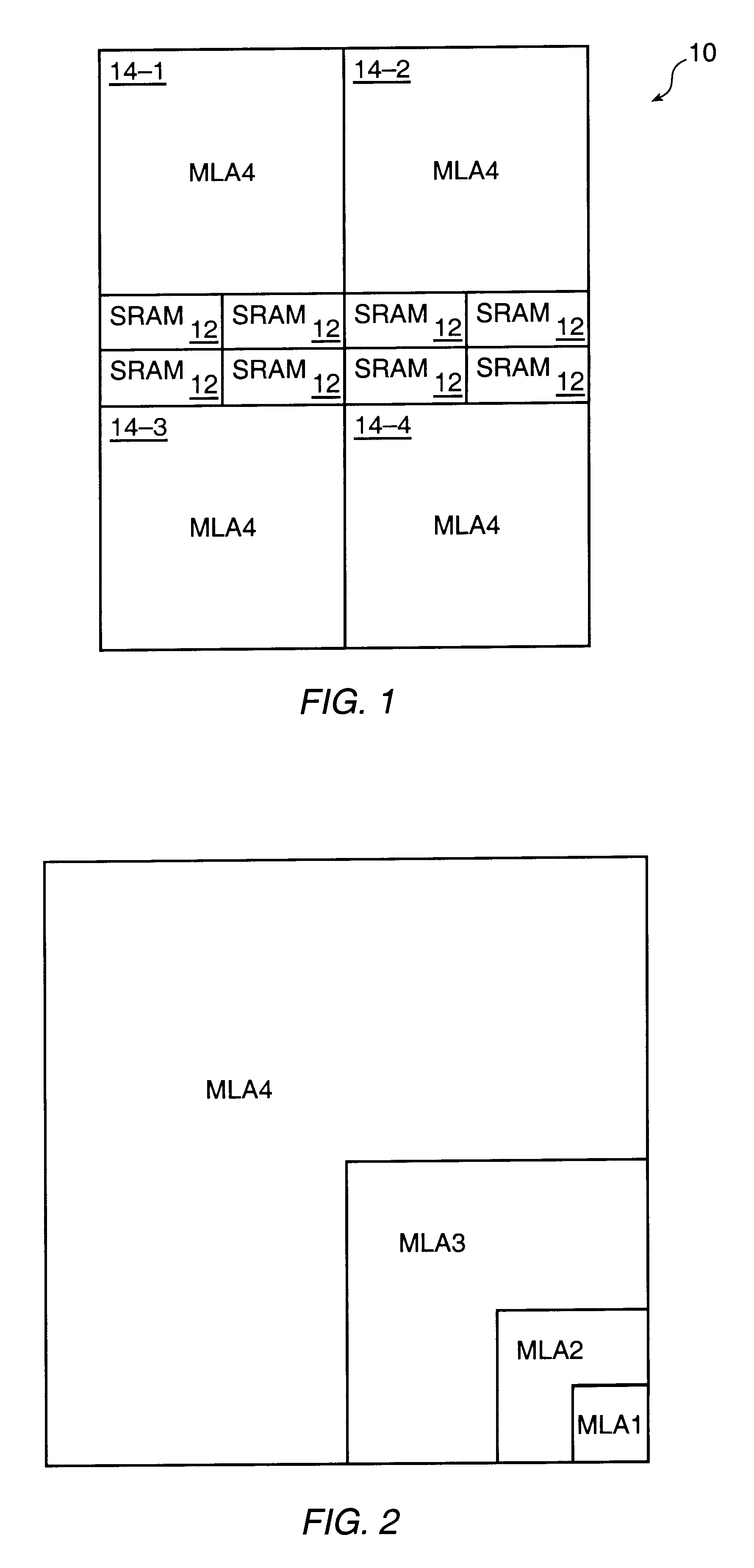
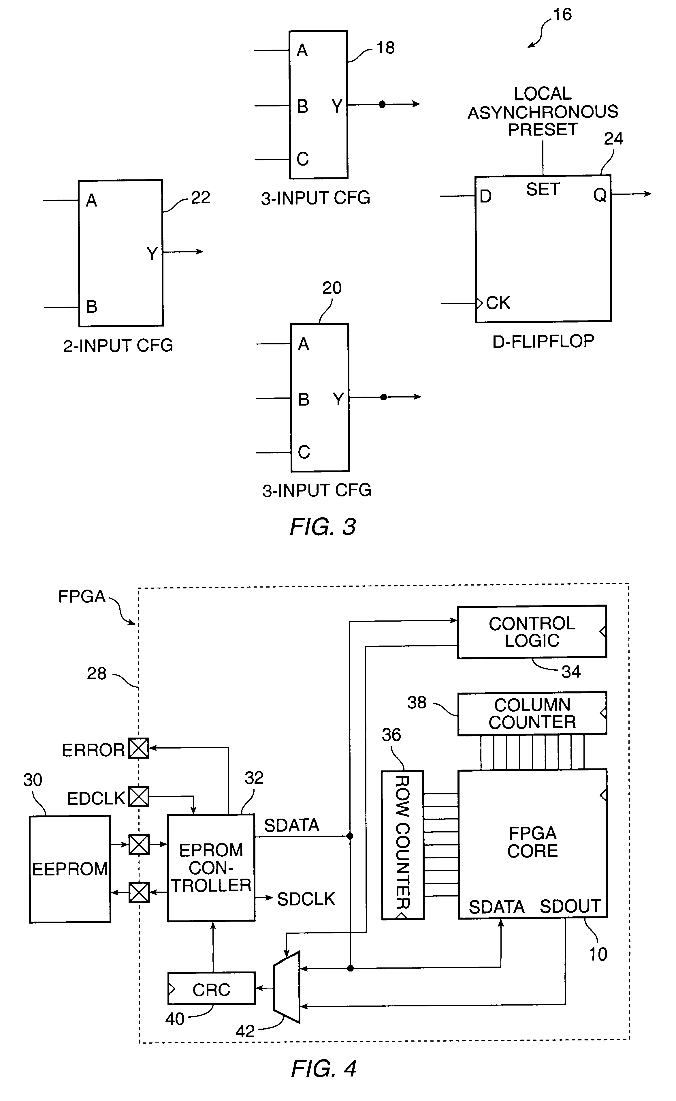
In an SRAM based FPGA, as discussed above, configuration SRAM hold the configuration data for programming the logic function modules, the interconnect architecture, and other known circuits in an FPGA. In the preferred embodiment, the programmable logic elements in the SRAM based FPGA are pass transistors controlled by the SRAM cells. It should be appreciated that the configuration SRAM is not grouped in a single location on the FPGA, but rather is distributed throughout the FPGA so that typically, the memory cells of the configuration SRAM are in close proximity to the devices the memory cells control.

In an SRAM based FPGA having both configuration SRAM and user-assignable SRAM, according to a first aspect of the present invention, cyclical ...


PUM


Abstract

A method for detecting an error in data stored in configuration SRAM and user assignable SRAM in a FPGA comprises the steps of providing a serial data stream into the FPGA from an external source, loading data from the serial data stream into the configuration SRAM in response to address signals generated by row column counters, loading data from the serial data stream into the user assignable SRAM in response to address signals generated by row and column counters, loading a seed and signature from the serial data stream into a cyclic redundancy checking circuit, cycling data out of the configuration SRAM and the user assignable SRAM by the row and column counters; performing error checking on the data that has been cycled out of the configuration SRAM and out of the user assignable SRAM by the cyclic redundancy checking circuit, and generating an error signal when an error is detected by the error checking circuit.

Description

1. Field of the InventionThe present invention relates to field programmable gate array (FPGA) integrated circuits having an array of logic modules and interconnect architecture configured by static random access memory (SRAM) cells disposed within the array of logic modules. More particularly, the present invention relates to cyclic redundancy checking (CRC) of the contents of the configuration SRAM for the logic modules and interconnect architecture in an FPGA.2. The Prior ArtOne manner known in the art for configuring the logic modules, interconnect and other circuits, such as input / output (I / O) circuits, in an FPGA is with data stored in SRAM cells distributed throughout the FPGA. The SRAM cells employed to configure the FPGA to implement the user-design are typically referred to as configuration SRAM. For reasons of reliability, it is important that the data in the configuration SRAM remains unchanged. Hence, one of the primary disadvantages in using configuration SRAM is that ...

Claims


Application Information

Patent Timeline
IPC IPC(8): G01R31/28G01R31/3185G06F11/10
CPCG01R31/318519G06F11/1004
Inventor PLANTS, WILLIAM C.
Owner MICROSEMI SOC
Why Eureka
Try Eureka