Manufacturing of cavity fuses on gate conductor level

Inactive Publication Date: 2001-08-14
INFINEON TECHNOLOGIES NORTH AMERICA CORPORATION +1
View PDF16 Cites 42 Cited by
  • Summary
  • Abstract
  • Description
  • Claims
  • Application Information

AI Technical Summary

Problems solved by technology

In some integrated circuits, conductive links are coupled to fuses, which may be cut or blown after fabrication using lasers or excessive current / voltage.
However, if the fuse link material is not sufficiently dispersed within the surrounding area, the fuse link may still represents a conductive path even after it is theoretically blown.

Method used


Image

  • Manufacturing of cavity fuses on gate conductor level
  • Manufacturing of cavity fuses on gate conductor level
  • Manufacturing of cavity fuses on gate conductor level

Examples


Embodiment Construction

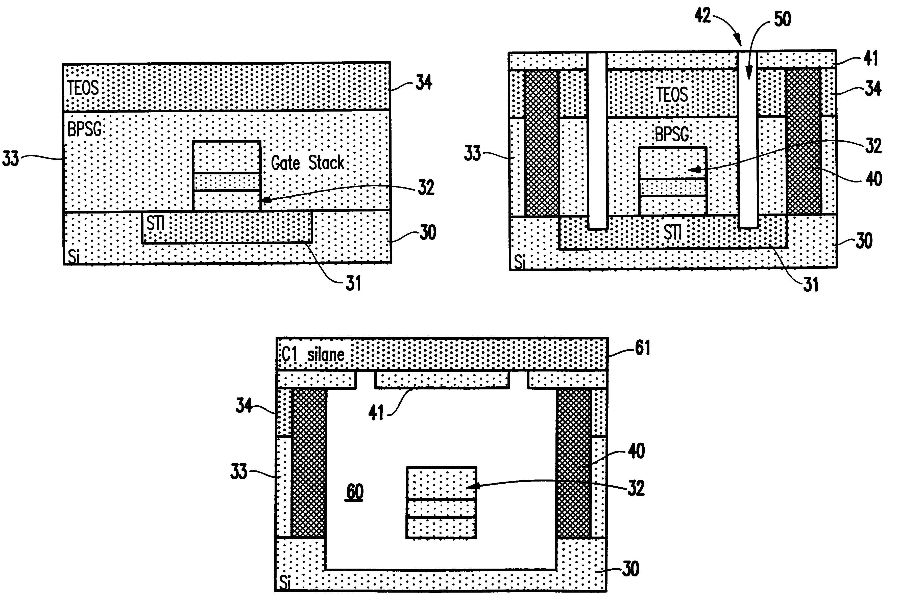
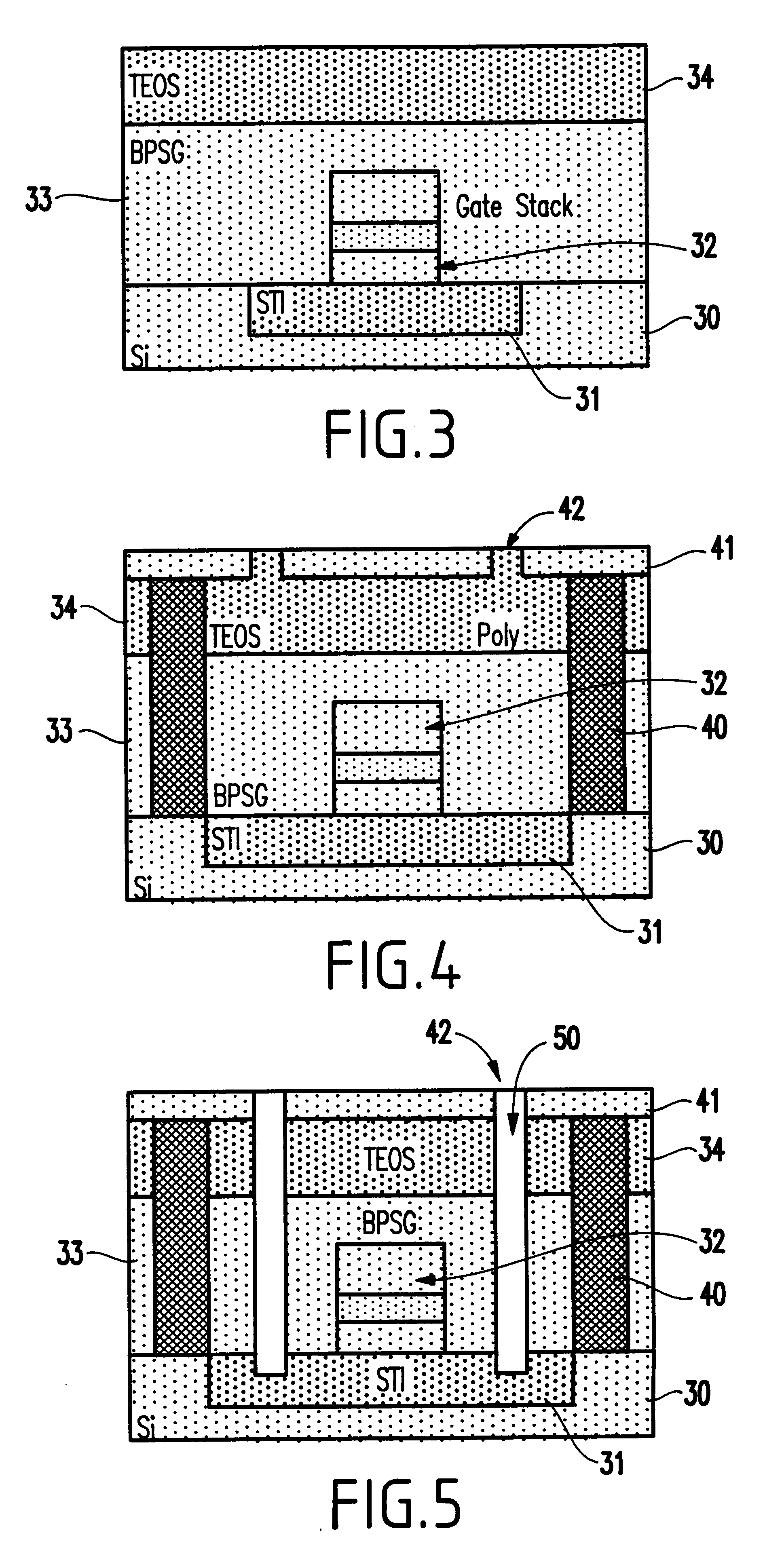
The invention, described in detail below, includes a unique method of forming a cavity around a gate conductor stack (which is utilized as a fuse link) and the associated unique structure. More specifically, with the invention wet etching of insulator layers surrounding the fuse link is performed through holes in the upper surface of the cavity region. This method simplifies the cavity formation process and allows much smaller integrated circuit features (such as gate stack structures which are utilized as fuse links) to include cavities.

Referring now to FIGS. 3-8, the method and structure of the invention will be explained in detail. More specifically, FIG. 3 illustrates a substrate 30 in which a shallow trench isolation (STI) region 31 has been formed. The substrate 30 could comprise any standard substrate, such as a silicon substrate and the shallow trench isolation region 31 could similarly comprise any conventional isolation material, such as tetraethylorthosilicate (TEOS), as ...


PUM


Abstract

A structure and method for making a cavity fuse over a gate conductor stack. The method includes providing a semiconductor substrate having a gate conductor stack over a shallow trench isolation region, forming oxide layers on the substrate about the gate conductor stack, etching electrical contact holes through the oxide layers to the substrate, filling the electrical contact holes with a first conductive material to establish electrical contact with the gate conductor stack, etching a pattern in an uppermost oxide layer of the oxide layers, depositing a conductive layer of a second conductive material over the oxide layers and the electrical contacts, planarizing the conductive layer whereby the conductive material remains only in the pattern, anisotropically etching the oxide layers to form at least one etching hole through the oxide layers to the shallow trench isolation region, and isotropically etching at least a portion of the oxide layers about the etching hole, whereby a cavity is formed beneath at least a portion of the conductive layer pattern, the gate conductor stack comprising a fuse.

Description

1. Field of the InventionThe present invention generally relates to fuses within semiconductor devices and more particularly to an improved method of forming a structure having a cavity around a gate stack conductor fuse.2. Description of the Related ArtSemiconductor integrated circuits (IC) and their manufacturing techniques are well known. In a typical integrated circuit, a large number of semiconductor devices may be fabricated on a silicon substrate. To achieve the desired functionality, a plurality of conductors are typically provided to couple selected devices together. In some integrated circuits, conductive links are coupled to fuses, which may be cut or blown after fabrication using lasers or excessive current / voltage.In a dynamic random access memory (DRAM) circuit, for example, fuses may be employed during manufacturing to protect some of the transistors' gate stacks from destruction due to inadvertent built-up of charges. Once fabrication of the IC is substantially compl...

Claims


Application Information

Patent Timeline
Patent Type & Authority Patents(United States)
IPC IPC(8): H01L23/52H01L23/525H01L21/82H01H69/02H01H85/00H01L21/8242H01L27/108
CPCH01L23/5256H01L23/5258H01L2924/3011H01L2924/0002H01L2924/00H01L21/82
Inventor ARNDT, KENNETH C.BRINTZINGER, AXEL C.CONTI, RICHARD A.COTE, DONNA R.NARAYAN, CHANDRASEKHARRAMACHANDRAN, RAVIKUMARRUPP, THOMAS S.SRINIVASAN, SENTHIL K.
Owner INFINEON TECHNOLOGIES NORTH AMERICA CORPORATION
Why Eureka
Try Eureka