
Method and system for testing cluster circuits in a boundary scan environment

a technology of boundary scan environment and cluster circuit, which is applied in the field of system and method for testing digital clusters on circuit boards, can solve the problems of increasing manual testing using an automatically controlled probe, insufficient physical size of the probe, and increasing the difficulty of individual circuit boards in a system made up of one or more circuit boards

Inactive Publication Date: 2002-04-23
LUCENT TECH INC
View PDF4 Cites 18 Cited by
  • Summary
  • Abstract
  • Description
  • Claims
  • Application Information

AI Technical Summary

Problems solved by technology

The testing of individual circuit boards in a system made up of one or more circuit boards is becoming more and more difficult due at least in part to the shrinking of the area between the components on the boards, and to the increasing complexity of the components and the interconnections between them on the board.
With this shrinking technology, manual testing using an automatically controlled probe is becoming more difficult.
In some cases, the probe is not small enough to physically contact the interconnections between the miniaturized circuit components.
Unfortunately, circuit boards in present systems are not formed in their entirety of boundary scan components.
The combination of boundary scan and cluster components presents a problem in testing the circuit board at the component level.
Since exhaustive functional testing is very expensive to implement, generally incomplete functional testing is performed to provide cost efficient manufacturing.
This incomplete functional testing results in a very low quality structural test and does not provide sufficient detail about which components are not operating properly, or which interconnection between components is faulty.
Thus, functional testing does not enable testing of the individual cluster circuit components and the interconnections between them and with the boundary scan components.
In the event that a circuit fails the functional test, no diagnosis can readily be performed to identify the faulty component or interconnection.
The functional test vectors are provided to the system by the designers, and cannot be generated automatically.
Furthermore, since functional testing does not require the identification of cluster components, a faulty component or interconnection between cluster components cannot be diagnosed for repair.

Method used


Image

  • Method and system for testing cluster circuits in a boundary scan environment
  • Method and system for testing cluster circuits in a boundary scan environment
  • Method and system for testing cluster circuits in a boundary scan environment

Examples


Embodiment Construction

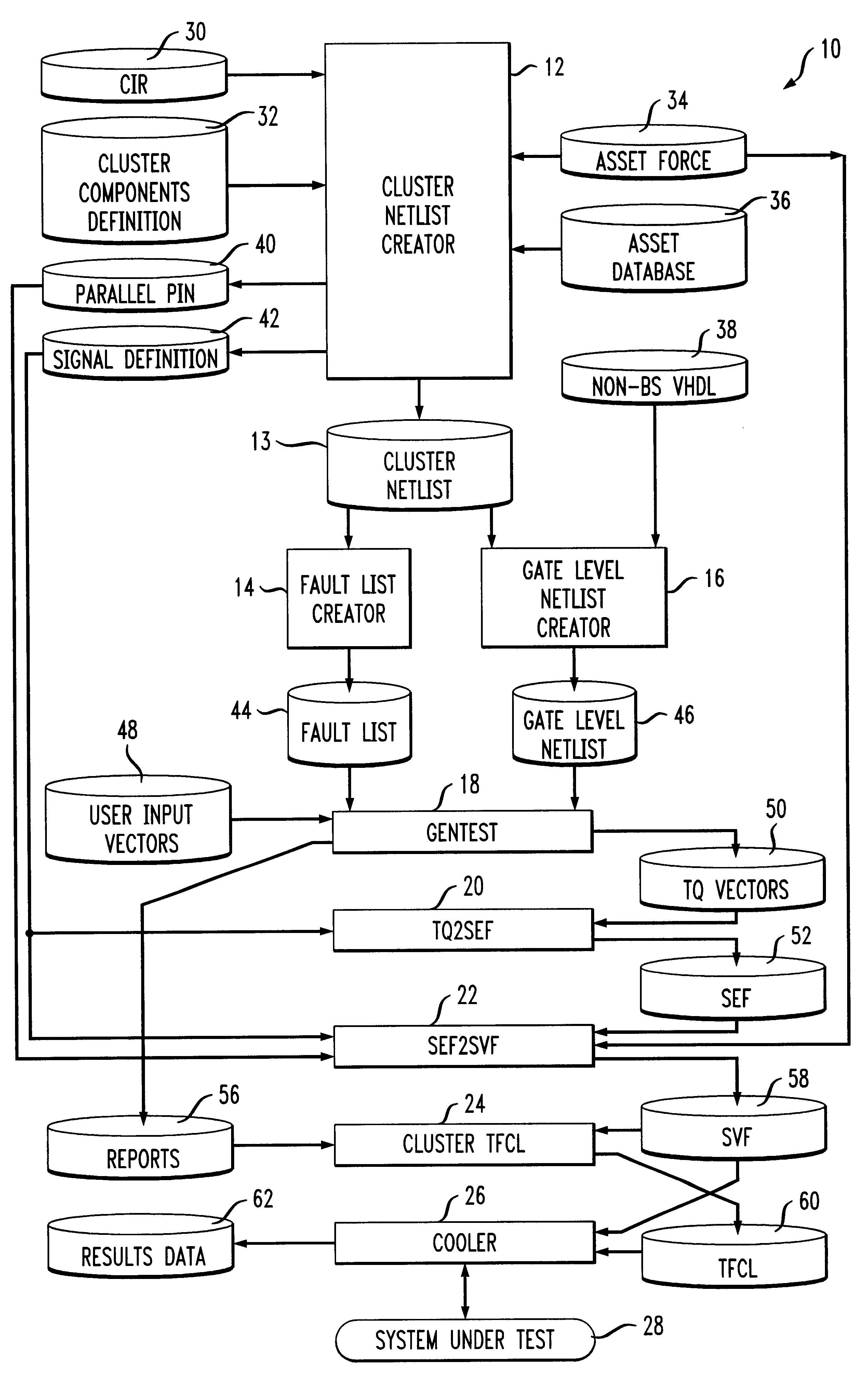
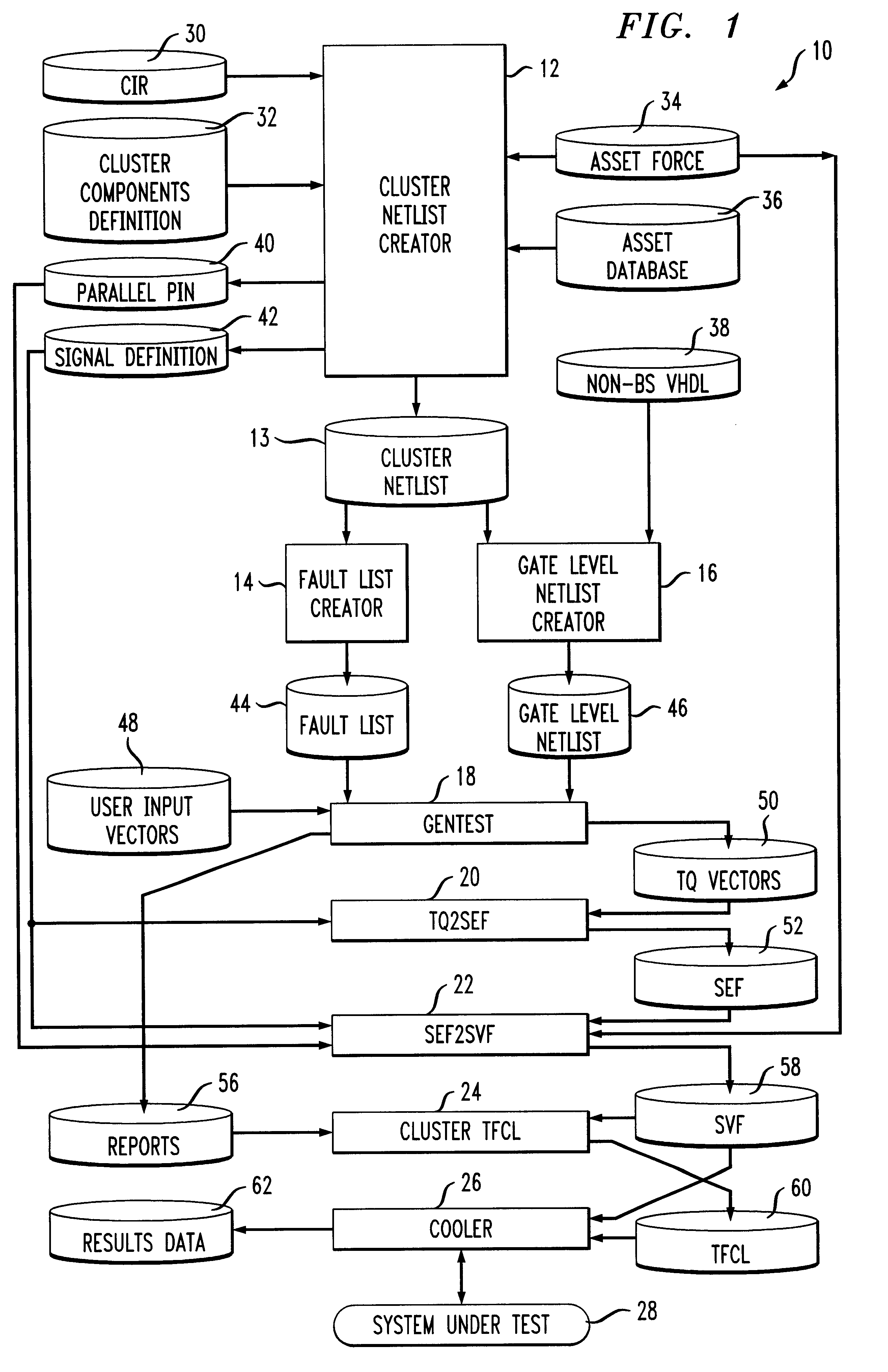
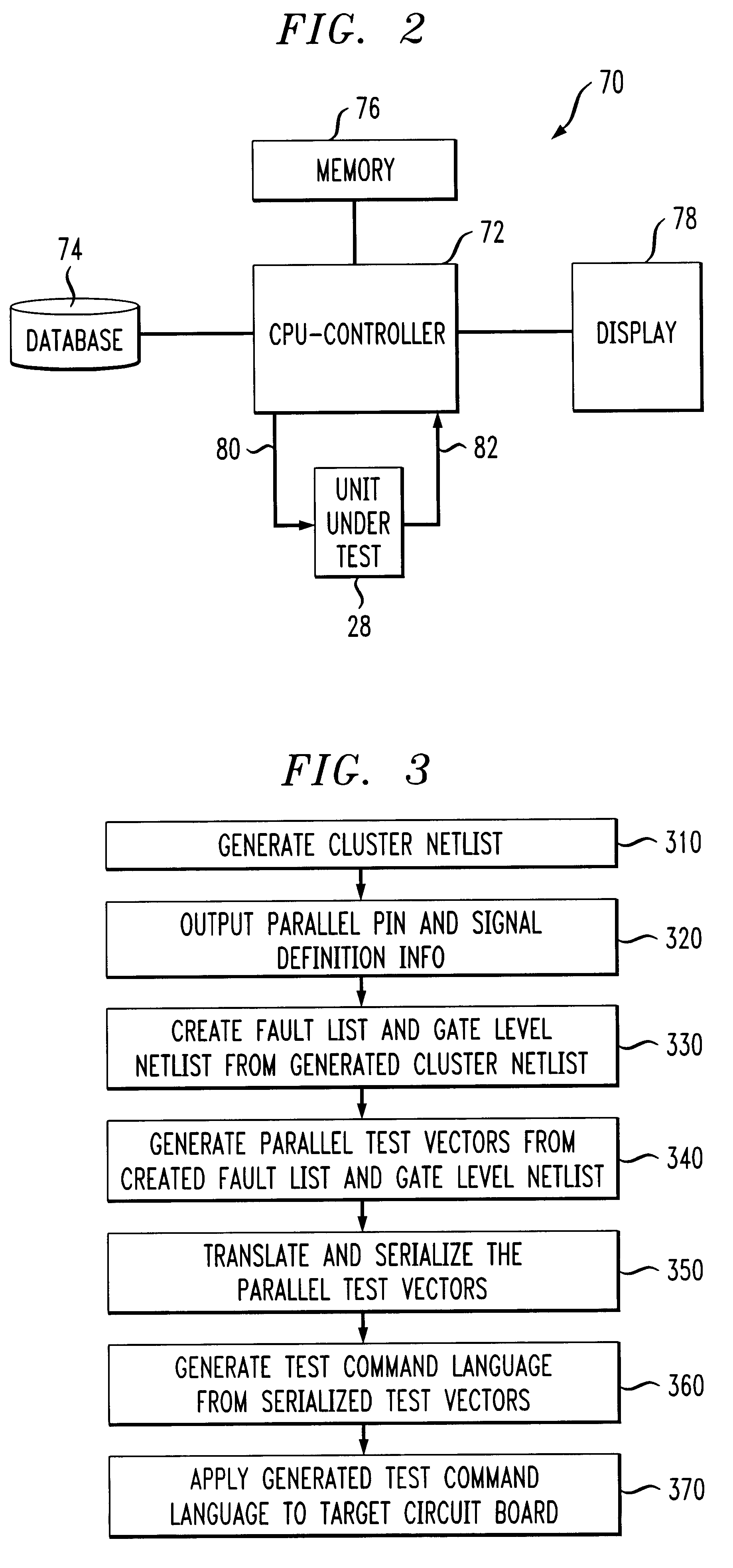
FIGS. 1 and 3 show the functional modules 10 and a method, respectively, for performing cluster tests in a boundary scan environment according to an embodiment of the present invention. Specifically, FIG. 1 shows the functional modules 10 which perform the various required tasks; FIG. 3 is a flow chart of the broad steps taken by an embodiment of the present invention. Circuit testing of this kind is generally performed in a computing environment having processors, memories, controllers, and a physical connection to the circuit board and / or particular elements on the circuit board (see FIG. 2). In FIG. 3, the first step 310 generates a cluster netlist representing the cluster portion of the circuit to be tested. In order to generate the cluster netlist, information relating to the circuit must be input into the system. For example, as shown in FIG. 1, the ASSET data base 36 supplies the Cluster Netlist Creator 12 with the complete boundary scan information relating to the board / circ...


PUM


Abstract

A method and system for testing circuit clusters in a boundary scan environment identifies the circuit clusters and corresponding neighboring boundary scan elements, and generates one or more test vectors to be applied to the cluster under test. The generated test vectors are serialized and input into an identified boundary scan element connected to the cluster being tested in the form of a boundary scan test chain. The output of the applied test vectors is observed from an output of another correspondingly identified boundary scan element connected to the cluster under test. During generation of test vectors a list of faults for detecting by each generated vector is maintained such that the observed output can be used to diagnose faults at the component level within the identified cluster.

Description

1. Field of the InventionThe present invention relates to testing electronic printed circuit or wiring boards and, more particularly, to a system and method for testing digital clusters on a circuit board in a boundary scan environment.2. Description of the Related ArtThe testing of individual circuit boards in a system made up of one or more circuit boards is becoming more and more difficult due at least in part to the shrinking of the area between the components on the boards, and to the increasing complexity of the components and the interconnections between them on the board. The reduction in size of components allows more components to fit onto each board, and thereby enables additional processing of information in less physical space than previously required.With this shrinking technology, manual testing using an automatically controlled probe is becoming more difficult. In some cases, the probe is not small enough to physically contact the interconnections between the miniatu...

Claims


Application Information

Patent Timeline
IPC IPC(8): G01R31/3183G01R31/28G01R31/3185
CPCG01R31/318307G01R31/318536G01R31/318561G01R31/318547G01R31/318544
Inventor CHAKRABORTY, TAPAN JYOTIVAN TREUREN, BRADFORD GENE
Owner LUCENT TECH INC
Learn More