Active pixel sensor with bootstrap amplification and reduced leakage during readout

a technology readout, which is applied in the field can solve the problems of sensitivity, noise, noise nature of active pixel sensor gain, and increase achieve the effect of reducing the amount of charge generated, and reducing the noise of the active pixel sensor

Inactive Publication Date: 2002-06-25
FOVEON
View PDF103 Cites 103 Cited by
  • Summary
  • Abstract
  • Description
  • Claims
  • Application Information

AI Technical Summary

Problems solved by technology

In the art of CMOS active pixel sensors, the sensitivity, noise, and nature of the gain of an active pixel sensor present issues of concern.
The readout amplifier in an active pixel sensor represents a substantial source of noise that in prior art pixel sensors has required design tradeoffs.
An increase in the area leads to an increase in the amount of charge generated.
One source of noise in an active pixel sensor is created by threshold fluctuations in the readout transistor.
As the size of the readout transistor is increased, the amount of threshold fluctuation, and hence the amount of noise decreases.
Junction leakage current is a dominant factor in the noise performance of many pixel sensors.
As pixel sensor size is scaled downward, electric field becomes a significant factor in junction leakage.

Method used


Image

  • Active pixel sensor with bootstrap amplification and reduced leakage during readout
  • Active pixel sensor with bootstrap amplification and reduced leakage during readout
  • Active pixel sensor with bootstrap amplification and reduced leakage during readout

Examples


first embodiment

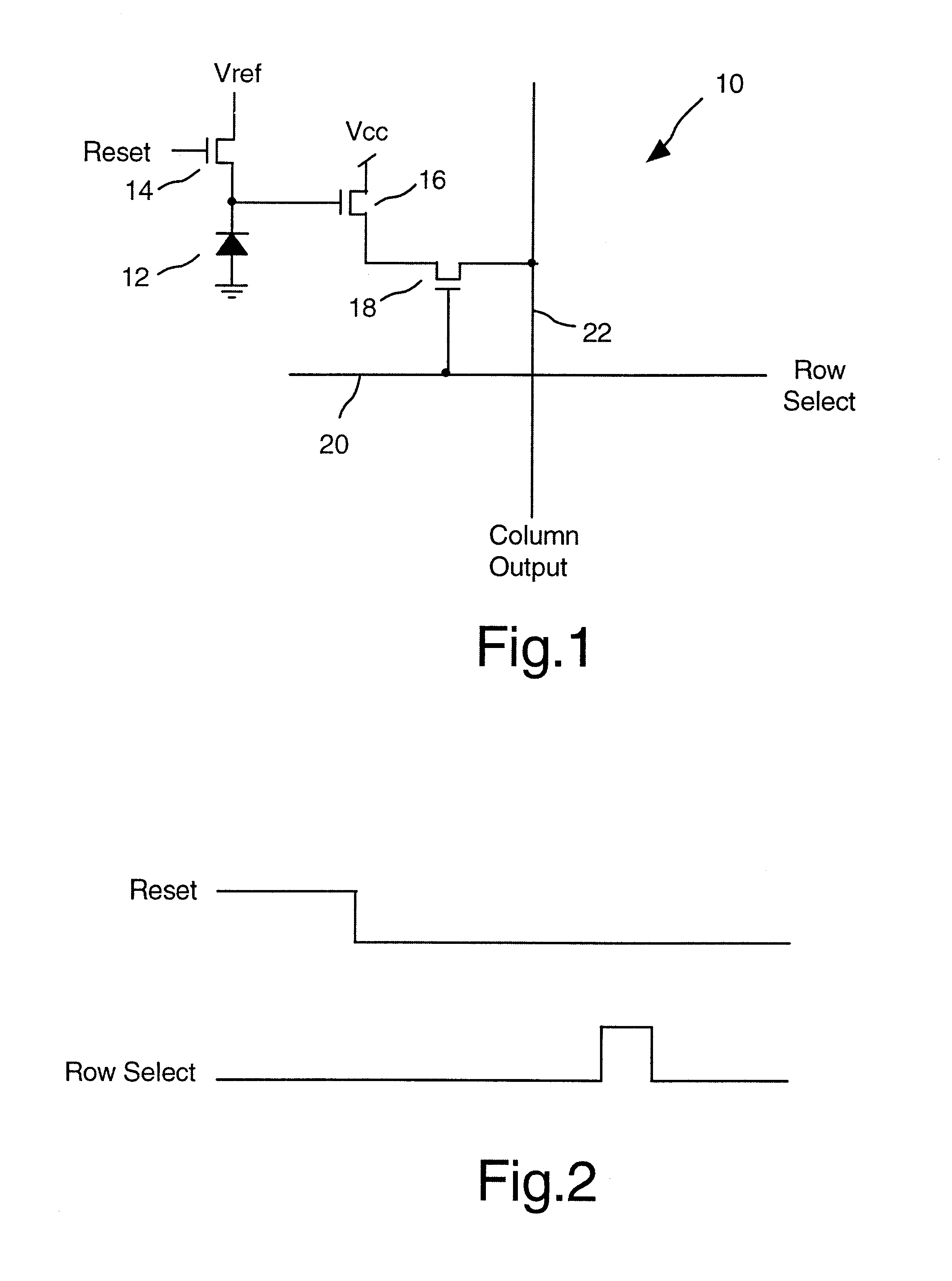
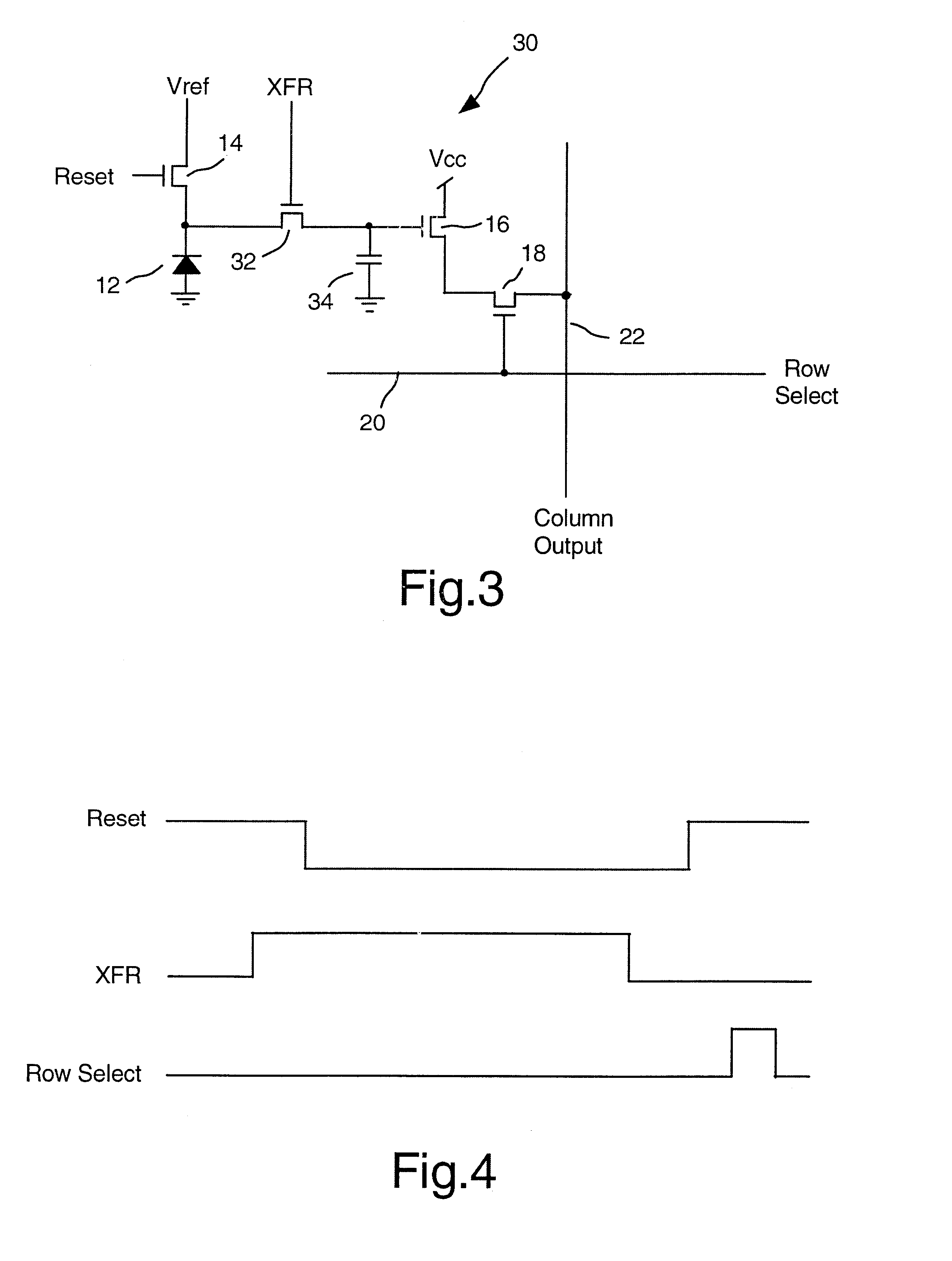
Referring now to FIG. 5, an active pixel sensor 50 according to the present invention is depicted schematically coupled to a row select line and a column output line. The active pixel sensor depicted 50 in FIG. 5 is similar to the active pixel sensor of 10FIG. 1, and accordingly, the same reference numerals are employed for corresponding elements in the two drawing figures. Thus active pixel sensor 50 includes photodiode 12 coupled in series with MOS N-Channel Reset transistor 14 between the fixed ground potential and the Vref voltage such that photodiode 12 is reverse biased. Active pixel sensor 50 of FIG. 3 differs from active pixel sensor 10 of FIG. 1 in the important aspect that the drain of the MOS N-Channel Source-Follower transistor 18 is connected to a switchable supply voltage Vd instead of a fixed drain supply voltage (Vcc in FIG. 1). Further, the voltage Vref may be a lower voltage than that encountered in the prior art.

second embodiment

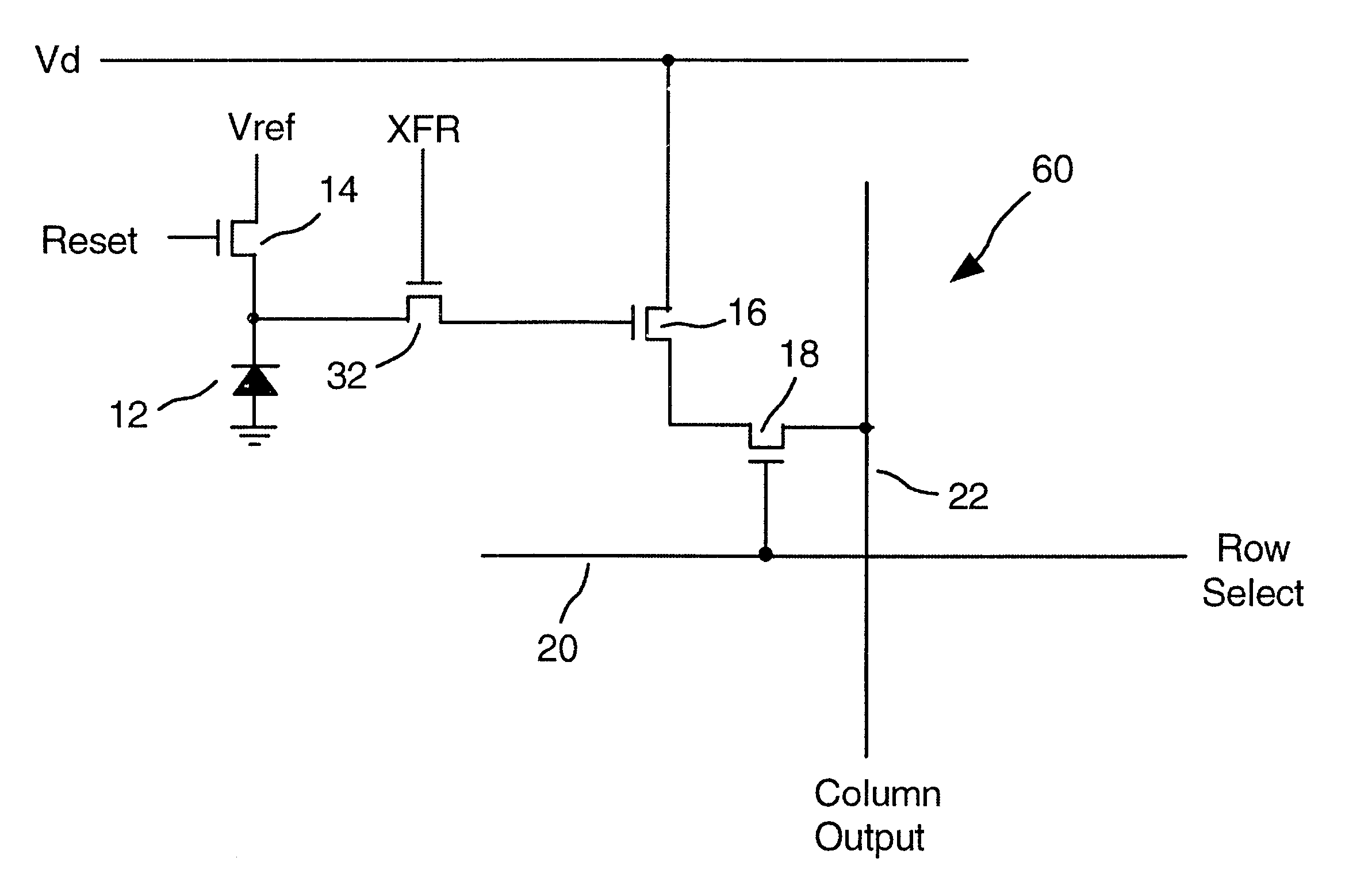
Referring now to FIG. 6, an active pixel sensor 60 according to the present invention is depicted schematically coupled to a row select line and a column output line. The embodiment of FIG. 6 is very similar to the embodiment of FIG. 5, except that MOS N-Channel Transfer transistor 32 is coupled between the cathode of photodiode 12 and the gate of MOS N-Channel Source-Follower transistor 16. The gate of MOS N-Channel Transfer transistor 32 is coupled to a XFR signal line.

The pixel sensors 50 and 60 of the present invention provides an improved performance in the environment of an array in which pixel sensors 50 or 60 is usually encountered. This aspect of the present invention may be most easily seen with reference to FIG. 7, a block diagram of a portion of an array including plurality of rows of active-pixel sensors of FIG. 5, and FIG. 6, a timing diagram illustrating the operation of an array of pixel sensors 50.

Array portion in FIG. 7 is shown as a 2.times.2 portion for illustrat...


PUM


Abstract

An integrated active pixel sensor array comprises a plurality of row select lines, each of said row select lines coupled to a source of a row-select signal; a plurality of source-follower drain row lines, each of said source-follower drain row lines coupled to a source of a source-follower drain row signal; a plurality of column output lines; a reset line coupled to a source of a reset signal; a source of reset potential; and a plurality of active pixel sensors, each pixel sensor associated with one row and one column of the array and including a photodiode having a first terminal coupled to a first reference potential and a second terminal, a Reset transistor having a gate coupled to the reset line, a drain coupled to the reset potential to reverse bias the photodiode, and a source coupled to the second terminal of the photodiode, a Source-Follower transistor having a gate coupled to the second terminal of the photodiode, a drain connected to the one of the plurality of source-follower drain row lines with which its active pixel sensor is associated, and a source, a Row-select transistor having a gate coupled to the one of the plurality of row-select lines with which its active pixel sensor is associated, a drain coupled to the source of the Source-follower transistor, and a source coupled to the one of the plurality of column output lines with which its active pixel sensor is associated.

Description

1. Field of the InventionThe present invention relates to active pixel sensors. More particularly, the present invention relates to variable biasing of several of the transistors in an active pixel sensor to improve sensitivity, reduce noise, to provide compressive non-linearity in the charge-to-voltage gain, and to reduce leakage current in pixels during readout.2. The Prior ArtIn the art of CMOS active pixel sensors, the sensitivity, noise, and nature of the gain of an active pixel sensor present issues of concern. The sensitivity of an active pixel sensor in measuring the charge generated by the photons striking the active pixel sensor is typically characterized by determining the volts generated per photon of light striking the active pixel sensor and is termed charge-to-voltage gain. The readout amplifier in an active pixel sensor represents a substantial source of noise that in prior art pixel sensors has required design tradeoffs. The gain in prior art active pixel sensors is...

Claims


Application Information

Patent Timeline
Patent Type & Authority Patents(United States)
IPC IPC(8): H01L27/146H04N3/15H04N5/357H04N5/369H04N5/374
CPCH04N3/155H04N5/374H04N5/3698H04N5/357H01L27/14609H04N25/60H04N25/709H04N25/76H04N25/745H01L27/146
Inventor MERRILL, RICHARD B.TURNER, RICHARD M.DONG, MILTON B.LYON, RICHARD F.
Owner FOVEON
Why Eureka
Try Eureka