Exposure apparatus, exposure method using the same and method of manufacture of circuit device

a technology of exposure apparatus and exposure method, which is applied in the direction of microlithography exposure apparatus, printers, instruments, etc., can solve the problems of reducing laser output, reducing laser output, and difficult chromatism of projection optical system upon illumination ligh

Inactive Publication Date: 2002-07-02
NIKON CORP
View PDF20 Cites 52 Cited by
  • Summary
  • Abstract
  • Description
  • Claims
  • Application Information

AI Technical Summary

Benefits of technology

In another aspect, the present invention has a further object to provide an improved measurement method for measuring a transmittance in an image projection region of the projection optical system or measuring an average illuminance or an irregularity of illuminance in the image projection region of the projection optical system. In a further aspect, the present invention has a still further object to provide a method for manufacturing a circuit device that can form a pattern image of a circuit device on the substrate always at an appropriate amount of exposing light and in a favorable imaging state.
With the configurations as described above, the present invention can expose the image of the device pattern to the substrate always at an optimal exposure amount and in a good imaging state, thereby enabling the production of the micro devices without reducing a yield rate of production, even if the transmittance of the projection optical system would vary.

Problems solved by technology

Moreover, in the case of use of quartz and fluorite for the projection exposure apparatus, achromatism in the projection optical system becomes difficult upon using illumination light.
From these reasons, the narrow-banded laser light source suffers from the disadvantages that a laser output is lowered as compared with a broad-band laser light source, and its life is shorter and its costs of production is more expensive than the broad-band laser light source.
Therefore, at this point of time, there is no way but using two kinds of glass materials, i.e. quartz and fluorite, for the refractive optical elements.
If such improvements could not be made, a throughput will be decreased due to an increase in a longer period of time for exposure.
A decrease in throughput is unacceptable, because it results in higher costs for the production of devices.
As a consequence, severe problems may occur that the transmittance of the projection optical system or the transmittance of the illumination optical system may fluctuate to a great extent for a relatively short period of time.
Such a great fluctuation of the transmittance results in a decrease in a precision for controlling the exposure amount to be provided on the photosensitive substrate, thereby deteriorating a fidelity of transcription of a fine pattern having a design line width of 0.25 to 0.12 micron to be transcribed on the substrate.
Therefore, the such conventional projection exposure apparatus suffers from the disadvantage in that no accurate control of the exposure amount can be performed because no fluctuation in the transmittance of the illumination optical system and the projection optical system behind the portion in the illumination light path is added thereto whatsoever, the portion in the illumination light path being the place where the intensity of the illumination light has been detected for controlling the exposure amount.
In addition, for the causes as described above, there is no assurance that the fluctuation in the transmittance of the projection optical system and the illumination optical system occurs in a uniform manner in the vision field on the image plane side of the projection optical system, so that there is the risk that irregularities of illuminance (or irregularities of the exposure amount) will occur against the projection optical system within the projection region of the pattern image conjugated with the illumination region of the illumination light on the reticle.
Furthermore, there is the concern about an occurrence of the disadvantage that imaging characteristics (e.g., distortion, spherical aberration, astigmatism, coma aberration, etc.) of the projection optical system may vary to a subtle extent, attendant upon an occurrence of such irregularities of illuminance or otherwise.
Therefore, in a projection exposure apparatus using such a laser light source, an error in controlling the exposure amount may occur due to a variation in the transmittance of the illumination optical system and the projection optical system.
Among those causes, in particular, the molecules of the impurities to be attached to the surface of the optical glass material may cause a decrease in an attenuation factor (transmittance or reflectance) in a monotonous way, if they are left non-removed and stayed as they are.
However, once the exposing energy is irradiated, they would be caused to be decomposed chemically and to disperse in a space.
This means to cause the entire attenuation factor (transmittance or reflectance) of the projection optical system and the illumination optical system to fluctuate, each being incorporated with a number of optical elements, and it is difficult to monitor a history of irradiation and the like and to predict characteristics of a variation in the attenuation factor (transmittance or reflectance).
Therefore, a conventional projection exposure apparatus using such an ArF laser light source has an error which may occur in controlling the exposure amount due to a variation in the attenuation factor (variation in transmittance or variation in reflectance) of the illumination system and the projection optical system.

Method used


Image

  • Exposure apparatus, exposure method using the same and method of manufacture of circuit device
  • Exposure apparatus, exposure method using the same and method of manufacture of circuit device
  • Exposure apparatus, exposure method using the same and method of manufacture of circuit device

Examples


first embodiment

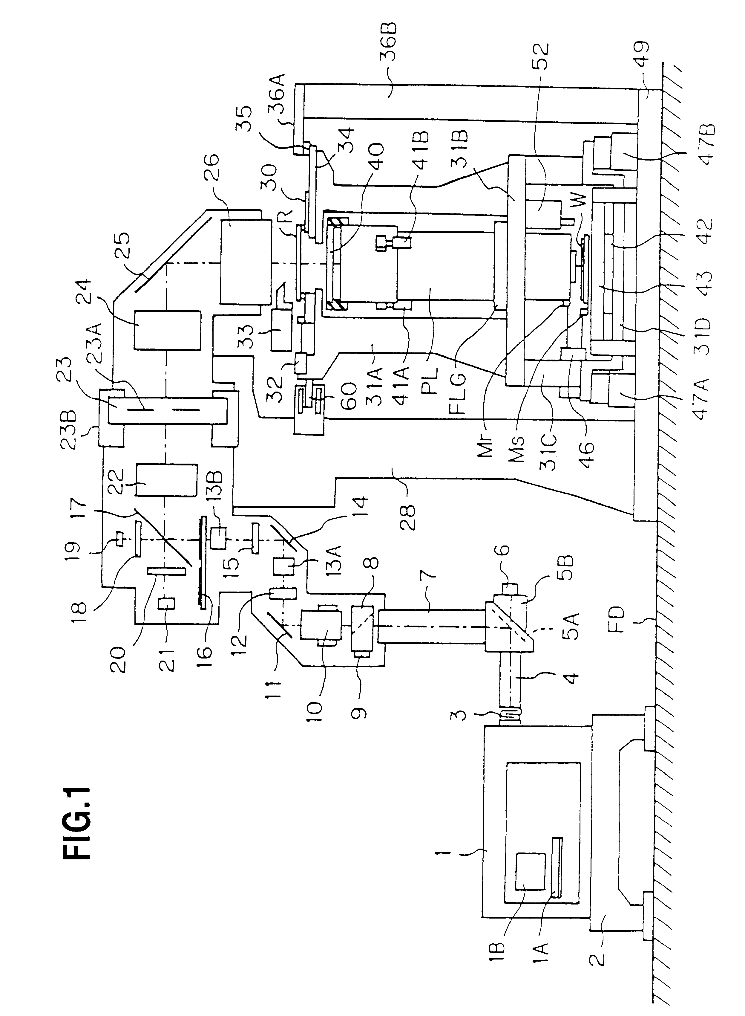
A description will be made of the overall construction of a projection exposure apparatus suitable for practicing the present invention with reference to FIG. 1. FIG. 1 shows a projection exposure apparatus of a step-and-scan type which is so adapted as to scan a semiconductor wafer W relative to a reticle R while projecting a circuit pattern of the reticle R onto the semiconductor wafer W through an projection optical system PL using an ArF excimer laser light source 1 which is narrowed so as to avoid an absorption band of oxygen between ranges of wavelengths of 192 nm to 194 nm.

As shown in FIG. 1, the main body of the ArF excimer laser light source 1 is equipped through a vibration proofing table 2 on a floor portion FD inside a clean room, or outside the clean room in some cases, of a semiconductor manufacture plant. The main body of the ArF excimer laser light source 1 is provided with a light source control system 1A for exclusive use, including an input unit such as, for examp...

second embodiment

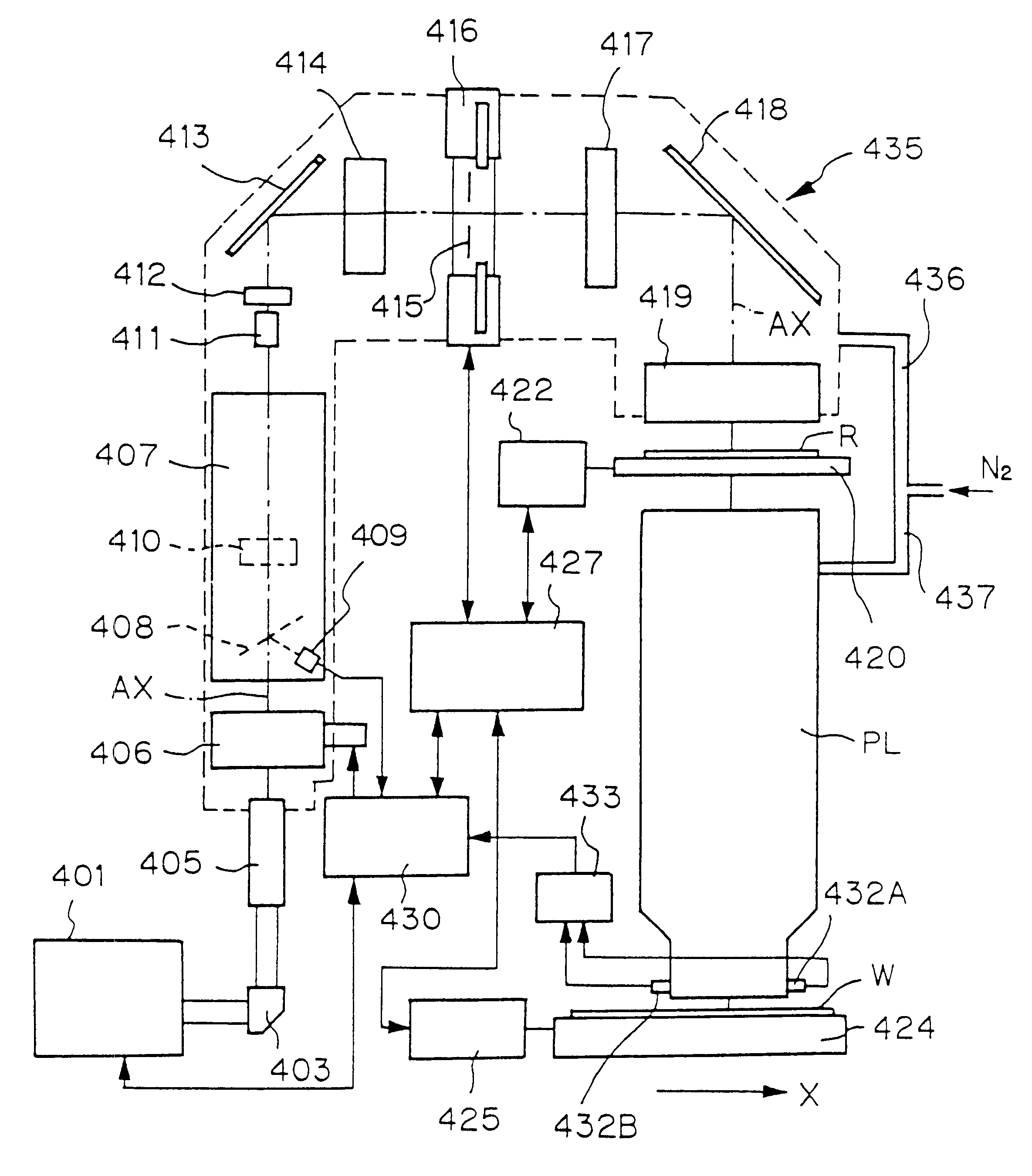
In the embodiment as shown in FIG. 25, transmittance data including both of the illumination optical system and the projection optical system PL is computed on the basis of a ratio of the intensity value of the illumination light detected by each of the detectors 432A and 432B to the intensity value of the original laser light energy, and the exposing conditions at the time of controlling the exposure amount are corrected in accordance with a variation in the transmittance data. The exposure amount, however, can also be controlled at a necessary degree of precision simply based on each of output signals from the detectors 432A and 432B, without using the photoelectric detector 409. Therefore, a device construction and operations necessary for this configuration will be described hereinafter as the present invention, with reference to FIG. 26.

FIG. 26 shows a relationship of the position of the tip end portion of the projection optical system PL with the position of the wafer stage 42...

third embodiment

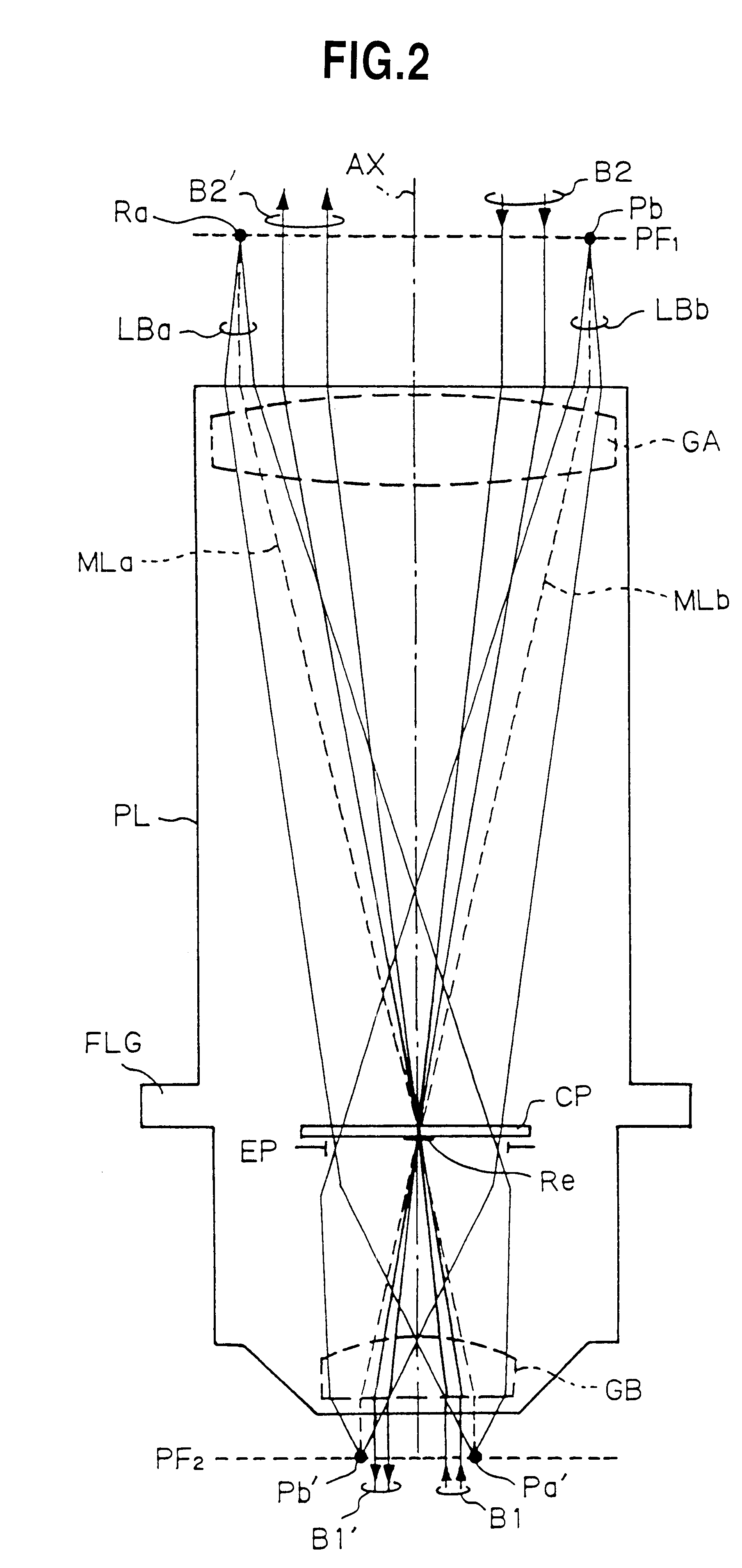
Then, a description will be made of the projection exposure apparatus according to the present invention suitable for use in practicing the present invention, with reference to the accompanying drawings. In this embodiment, the present invention is applied to a scanning type projection exposure apparatus of a step-and-scan type, which uses a projection optical system of a reflection-refraction type as a projection optical system.

FIG. 29 shows a brief configuration of the projection exposure apparatus of this embodiment. In FIG. 29, illumination light IL composed of pulse laser light emitting from an excimer laser light source 502 with its emission state controlled by an exposure control unit 501 is deviated by an eccentric mirror 503 and reaches a first illumination system 504. As the excimer laser light source 502 in this embodiment, there may be used a broad-banded laser light source of a KrF excimer laser (wavelength of 193 nm) with a half value width of an oscillating spectrum m...


PUM

PropertyMeasurementUnit
wavelengthaaaaaaaaaa
central wavelengthaaaaaaaaaa

Abstract

An exposure method for irradiating a mask with an illumination light through an illumination optical system and exposing photosensitive substrate to the illumination light through a projection optical system including the steps of supplying gas having less absorption of the illumination light to a light path of the illumination light, at least a portion of the illumination optical system and the projection optical system; and changing an exposing condition for the photosensitive substrate in accordance with a variation in transmittance or in reflectance of at least one of the illumination optical system and the projection optical system, resulting from irradiation of the illumination light and attenuation of the illumination light in the light path.

Description

The present invention relates to an exposure apparatus for use in a lithography process in a production line for manufacturing semiconductor devices, liquid crystal display devices and an exposure method using such exposure apparatus. The present invention also relates to a method for manufacturing circuit devices for use in forming electronic circuit devices on a semiconductor substrate (wafer), glass substrate, and so on.BACKGROUND TECHNOLOGYRecently, at plants for manufacturing semiconductor devices such as super LSIs and so on, developments for mass-producing D-RAMs (memory chips), processor chips and the like, having a degree of integration and a fineness of a class of 256 Mbits on a large scale have been carried out extensively with great effort. As developments advance, exposure apparatuses for use in a next-generation lithography process (representatives being processes for coating a resist, exposing, developing resist, etc.) are also required to have a higher precision of a...

Claims


Application Information

Patent Timeline
Patent Type & Authority Patents(United States)
IPC IPC(8): G03F7/20
CPCG03F7/70058G03F7/70066G03F7/70225G03F7/70241G03F7/70258G03F7/70358G03F7/70558G03F7/70591G03F7/7085G03F7/70941G03F7/20
Inventor NISHI, KENJIKIUCHI, TORU
Owner NIKON CORP
Why Eureka
Try Eureka