
Off-concentric polishing system design

a polishing system and polishing technology, applied in the direction of grinding machines, manufacturing tools, lapping machines, etc., can solve the problems of affecting yield and chip performance, difficult, if not impossible, to find substantial rotational optimization between the platen and the carrier, and the difficulty in achieving uniform polishing of the wafer, etc., to achieve the effect of removing the desired thickness of the semiconductor wafer

Inactive Publication Date: 2002-08-13
IBM CORP
View PDF8 Cites 42 Cited by
  • Summary
  • Abstract
  • Description
  • Claims
  • Application Information

AI Technical Summary

Benefits of technology

In a final aspect, the present invention is directed to a method of polishing a semiconductor wafer comprising the steps of: (a) providing a polishing tool comprising at least two polishing platens, the platens being positioned adjacent to each other such that polishing portions of the platens are substantially co-planar; and at least one wafer carrier movably mounted adjacent the platens such that one or more semiconductor wafers mounted to the carrier may be polished by the at least two platens substantially simultaneously; (b) providing at least one semiconductor wafer in need of polishing; (c) contacting the semiconductor wafer to the polishing platens; (d) polishing the semiconductor wafer; and (e) removing a desired thickness of the semiconductor wafer.

Problems solved by technology

As more layers are built up on the silicon wafer, problems caused by surface non-planarity become increasingly severe and can impact yield and chip performance.
As there are a limited number of variables to work with, it is difficult, if not impossible, to find substantial rotational optimization between the platen and the carrier.
Another disadvantage with prior art CMP tool configuration is the difficulty in achieving uniform polishing of the wafers due to the conventional distribution of slurry under the wafer during polishing.
Conventional slurry delivery systems, while providing adequate amounts of slurry to the wafer edge, do not deliver enough slurry to the wafer center.
Non-uniform slurry delivery is further exacerbated by the tool configuration because the wafer carrier is substantially disposed over the polishing tool.
Thus, the inadequate slurry delivery results in non-uniform polishing which leads to defects on the wafer surface.
Still another disadvantage of the prior art polishing tools is the inability to provide more than one polishing application at a time.
For example, if a unique surface required polishing with polishing pads of different textures, the polishing must be performed sequentially by multiple polishing steps which is very costly and non-manufacturable.
Furthermore, the necessity for multiple, sequential polishing steps require that more than one polishing tool be placed inside the clean room used during wafer manufacture taking up valuable space.
A further disadvantage of the prior art is the cumbersome in-situ methods to detect the planarization endpoint of the films on the semiconductor wafer.
Since the wafer carrier is typically positioned face down over the polishing platen, it is difficult and time consuming to determine the endpoint of the film being polished without stopping the polishing process to make a determination.
However, these in-situ methods are subject to the corrosive effects of the slurry and the quality of the detected signal is diminished since a direct measurement is not possible.

Method used


Image

  • Off-concentric polishing system design
  • Off-concentric polishing system design
  • Off-concentric polishing system design

Examples


Embodiment Construction

)

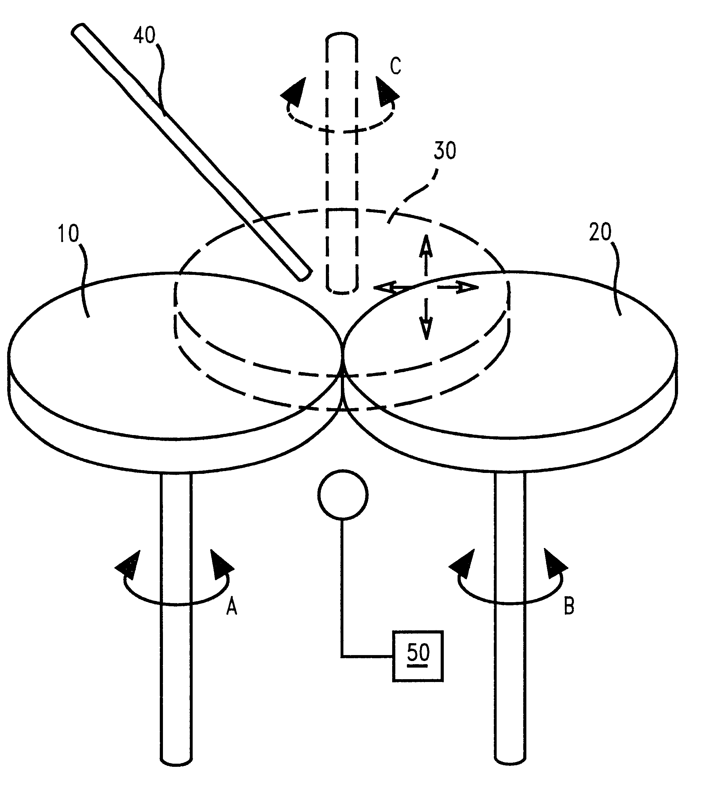
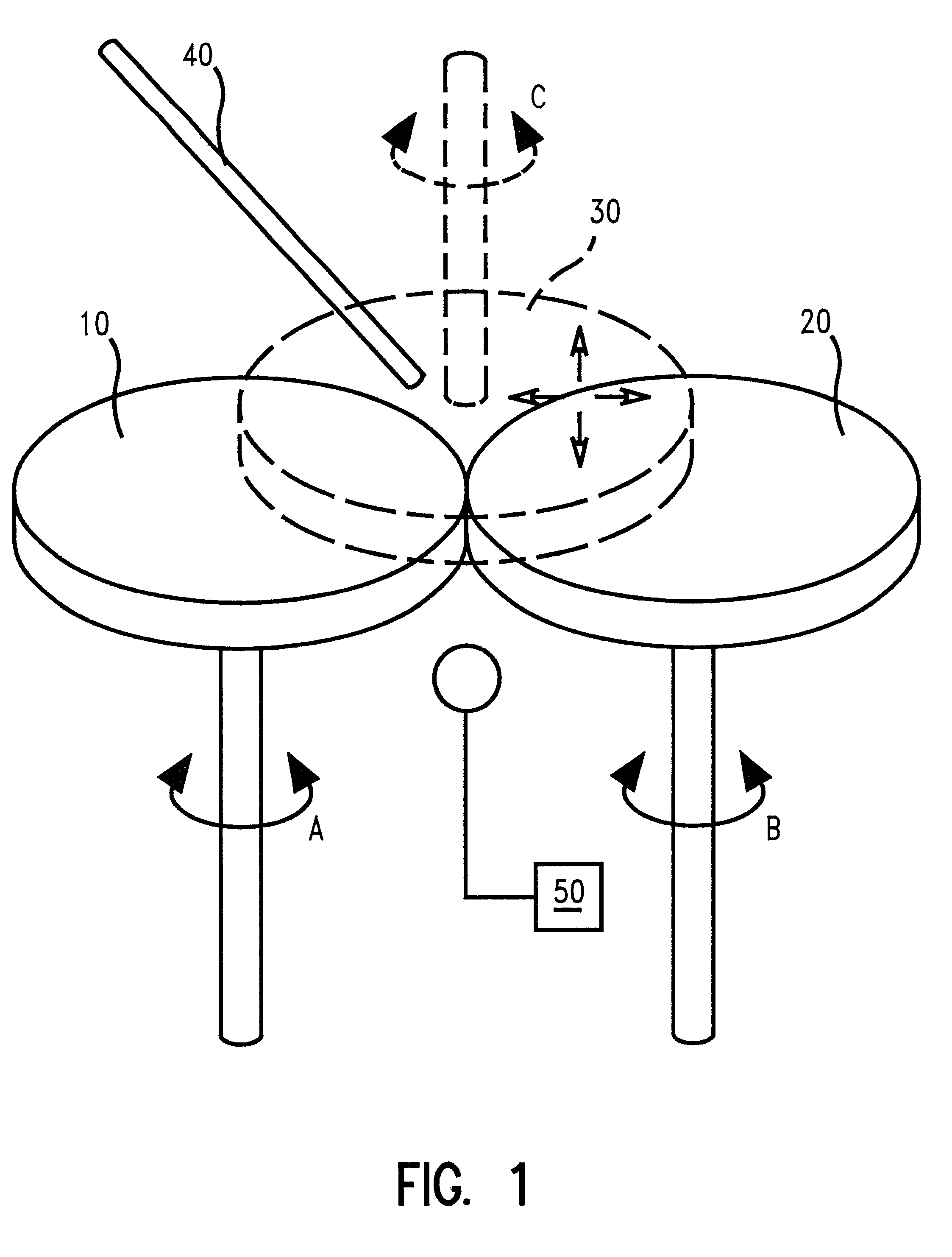
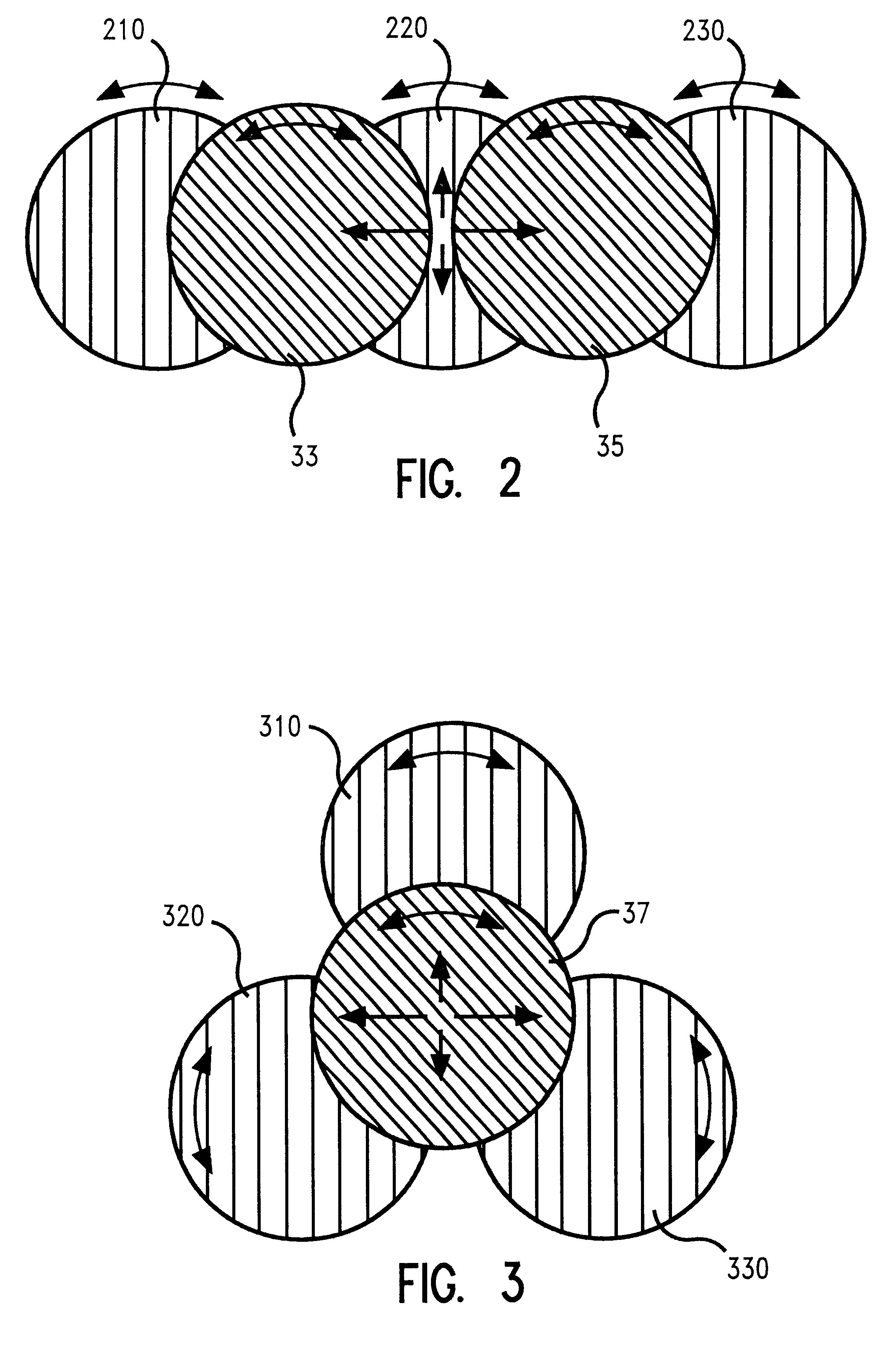
In describing the preferred embodiment of the present invention, reference will be made herein to FIGS. 1-6 of the drawings in which like numerals refer to like features of the invention. Features of the invention are not necessarily shown to scale in the drawings.

The present invention discloses an off-concentric CMP tool having multiple polishing platens, e.g., at least two polishing platens. The off-concentric nature of the present invention provides a platen configuration wherein a wafer carrier holding a semiconductor wafer for polishing is disposed over at least two platens substantially similar in size to the wafer and positioned adjacent to each other such that the wafer may be polished by more than one platen simultaneously.

Surprisingly, utilizing multiple platens in the off-concentric configuration of the present invention provides additional variables for optimizing uniformity of planarization. Polishing an object, such as a semiconductor wafer, utilizing multiple platens...


PUM


Abstract

An apparatus and method of planarizing objects, particularly electronic components. The off-concentric polishing system of the present invention comprises at least two polishing platens positioned adjacent each other such that the polishing portions of the platens are substantially co-planar. At least one wafer carrier is moveably mounted over the at least two platens such that a wafer may be polished by more than one platen substantially simultaneously. The platen configurations may be in a linear or non-linear configuration such that the wafer being polished is no longer centrally disposed over a single platen but is off-concentrically positioned over multiple platens. The off-concentric positioning of the wafer provides enhanced slurry distribution and endpoint detection. The present invention reduces time and cost in manufacturing electronic components by engaging several polishing conditions simultaneously without the need for sequential polishing.

Description

1. Field of the InventionThis invention is directed to a method and apparatus for chemical mechanical polishing, particularly in the manufacture of semiconductor wafers.2. Description of Related ArtFabrication of semiconductor integrated circuits (IC) is a complicated multi-step process for creating microscopic structures with various electrical properties to form a connected set of devices. As the level of integration of ICs increases, the devices become smaller and more densely packed, requiring more levels of photolithography and more processing steps. As more layers are built up on the silicon wafer, problems caused by surface non-planarity become increasingly severe and can impact yield and chip performance. During the fabrication process, it may become necessary to remove excess material in a process referred to as planarization.Chemical mechanical polishing (CMP) is well known in the art as a planarization technique in the manufacture of semiconductor wafers. CMP involves the...

Claims


Application Information

Patent Timeline
Patent Type & Authority Patents(United States)
IPC IPC(8): B24B27/00B24B37/04
CPCB24B27/0076B24B37/042
Inventor HUYNH, CUC K.MANFREDI, PAUL A.MARTIN, THOMAS J.NADEAU, DOUGLAS P.WU, YUTONG
Owner IBM CORP
Features
  • Generate Ideas
  • Intellectual Property
  • Life Sciences
  • Materials
  • Tech Scout
  • Unparalleled Data Quality
  • Higher Quality Content
  • 60% Fewer Hallucinations
Learn More