Structure of stacked integrated circuits

a technology of integrated circuits and structures, applied in the direction of electrical equipment, semiconductor devices, semiconductor/solid-state device details, etc., can solve the problems of difficult to make small, thin, light products, and the above-mentioned structure has the disadvantages

Inactive Publication Date: 2002-08-27
KINGPAK TECH INC
View PDF2 Cites 90 Cited by
  • Summary
  • Abstract
  • Description
  • Claims
  • Application Information

AI Technical Summary

Benefits of technology

It is therefore another object of the invention to provide a structure of stacked integrated circuits and method for manufacturing the same in which the stacking processes can be simplified because an isolation layer can be simultaneously formed on the integrated circuit when coating the adhesive layer.
According to this structure, the lower integrated circuit is free from being pressed and damaged by the upper integrated circuit when stacking a plurality of integrated circuits. Thus, the stacking processes can be facilitated and the manufacturing costs can also be lowered.

Problems solved by technology

Because the area of the circuit board is limited, it is not possible to increase the number of the integrated circuits mounted on the circuit board.
Therefore, it is difficult to make the products small, thin, and light.
However, the above-mentioned structure has the disadvantages described hereinbelow.
As a result, the manufacturing processes are complicated, and the manufacturing costs are high.
Thus, no other apparatus should be prepared for manufacturing the stacked integrated circuits.

Method used


Image

  • Structure of stacked integrated circuits
  • Structure of stacked integrated circuits

Examples


Embodiment Construction

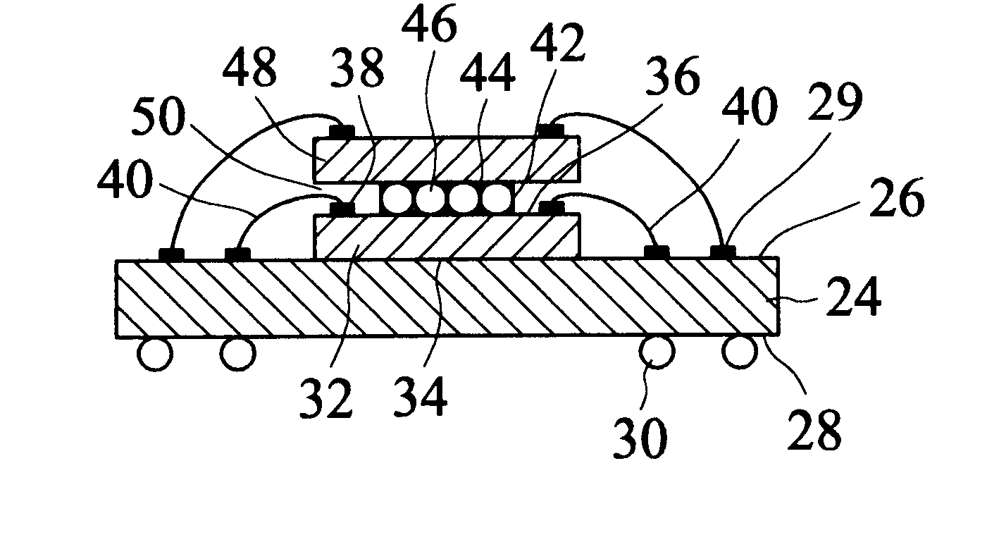
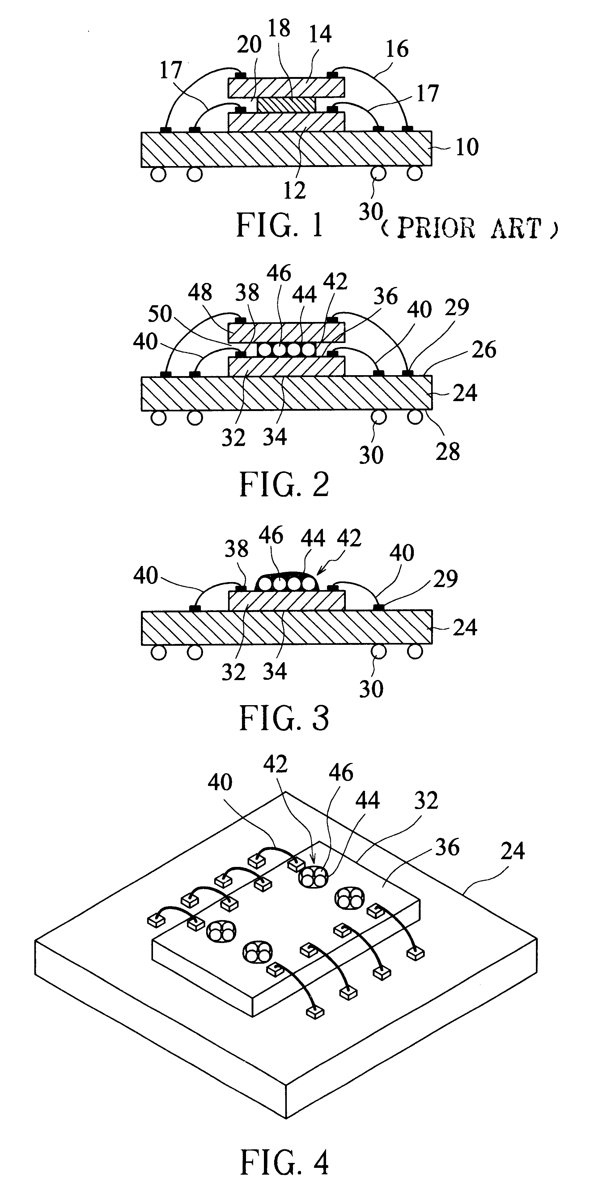
Referring to FIG. 2, the structure of stacked integrated circuits according to the invention includes a substrate 24, a lower integrated circuit 32, a plurality of wirings 40, an adhesive layer 42, and an upper integrated circuit 48.

The substrate 24 has a first surface 26 and a second surface 28. The first surface 26 is formed with signal input terminals 29 for transmitting the signals from the integrated circuit to the substrate 24. The second surface 29 is formed with signal output terminals 30 for transmitting the signals from the integrated circuit to the circuit board (not shown). The signal output terminals 30 can be connected to a plurality of metallic balls 30 arranged in the form of a ball grid array (BGA).

The lower integrated circuit 32 has a first surface 34 and a second surface 36. The first surface 34 is adhered onto the first surface 26 of the substrate 24. The second surface 36 is formed with a plurality of bonding pads 38 for electrically connecting to the substrate ...


PUM


Abstract

The structure of stacked integrated circuits includes a substrate, a lower integrated circuit, a plurality of wirings, an adhesive layer, and an upper integrated circuit. The substrate has a first surface formed with signal input terminals, and a second surface formed with signal output terminals. The lower integrated circuit has a first surface and a second surface. The first surface is adhered to the first surface of the substrate while the second surface is formed with a plurality of bonding pads. The wirings have first ends and second ends. The first ends are electrically connected to the bonding pads of the lower integrated circuit while the second ends are electrically connected to the signal input terminals of the substrate. The adhesive layer is coated on the second surface of the lower integrated circuit and includes adhesive agent and filling elements. The upper integrated circuit is stacked above the second surface of the lower integrated circuit with the adhesive layer inserted between the upper and lower integrated circuit. The lower integrated circuit is adhered to the upper integrated circuit by the adhesive agent. A predetermined gap is formed between the lower and upper integrated circuit by the filling elements. According to this structure, the wirings located under the lower integrated circuit are free from being pressed and damaged by the upper integrated circuit when stacking a plurality of integrated circuits. Thus, the stacking processes can be facilitated and the manufacturing costs can also be lowered.

Description

1. Field of the InventionThe invention relates to a structure of stacked integrated circuits and method for manufacturing the same, in particular, to a structure of stacked integrated circuits in which integrated circuits can be effectively stacked so as to facilitate the manufacturing processes.2. Description of the Related ArtIn the current technological field, every product needs to be light, thin, and small. Therefore, it is preferable that the integrated circuit has a small volume in order to meet the demands of the products. In the prior art, even if the volumes of integrated circuits are small, they only can be electrically connected to the circuit board in parallel. Because the area of the circuit board is limited, it is not possible to increase the number of the integrated circuits mounted on the circuit board. Therefore, it is difficult to make the products small, thin, and light.To meet the demands of manufacturing small, thin, and light products, a lot of integrated circ...

Claims


Application Information

Patent Timeline
Patent Type & Authority Patents(United States)
IPC IPC(8): H01L21/02H01L25/065H01L21/58
CPCH01L24/29H01L24/32H01L24/83H01L25/0657H01L2224/32145H01L2224/48091H01L2224/48227H01L2224/73265H01L2224/8319H01L2224/8385H01L2225/0651H01L2225/06575H01L2924/01075H01L2924/07802H01L2924/14H01L2924/15311H01L2924/00014H01L2924/01033H01L2224/83139
Inventor CHEN, WEN CHUANPENG, KUO FENGWU, JICHENCHANG, CHIA JUNG
Owner KINGPAK TECH INC
Why Eureka
Try Eureka