Semiconductor device having a library of standard cells and method of designing the same

a technology of standard cells and semiconductor devices, which is applied in the direction of semiconductor devices, semiconductor/solid-state device details, electrical apparatus, etc., can solve the problems of deterioration of transistor characteristics, metal wiring lines, and mos transistor t1 or t2 gate oxide film being liable to be damaged by electrons

Inactive Publication Date: 2003-01-07
RENESAS ELECTRONICS CORP
View PDF18 Cites 130 Cited by
  • Summary
  • Abstract
  • Description
  • Claims
  • Application Information

AI Technical Summary

Problems solved by technology

In that case, the gate oxide film of the MOS transistor T1 or T2 is liable to be damaged by electrons launched from a plasma into the metal wiring line during wafer processing such as an etching of the metal wiring line or a removal of the resist.
This eventually has resulted in a deterioration of the transistor characteristics.

Method used


Image

  • Semiconductor device having a library of standard cells and method of designing the same
  • Semiconductor device having a library of standard cells and method of designing the same
  • Semiconductor device having a library of standard cells and method of designing the same

Examples


first embodiment

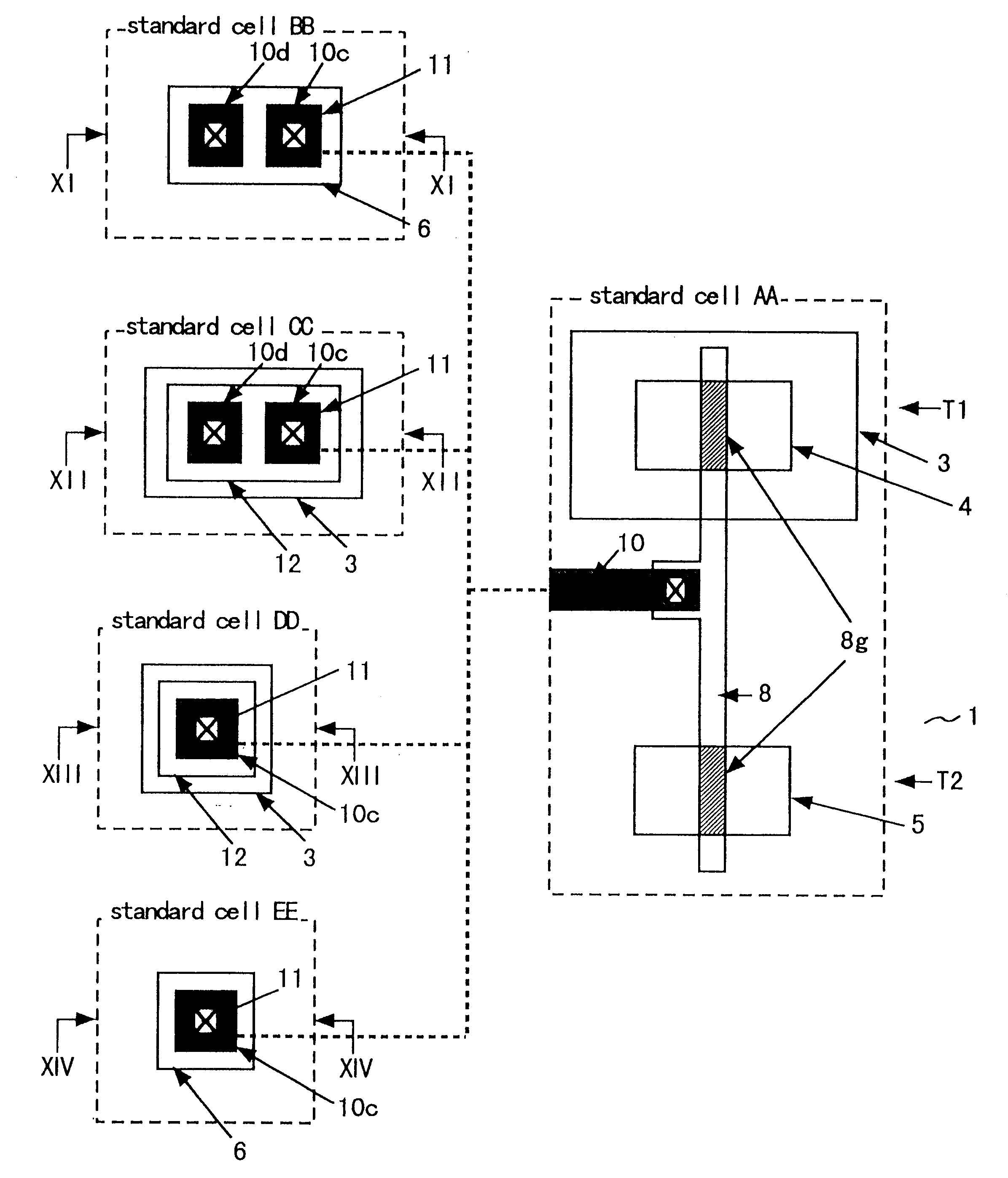
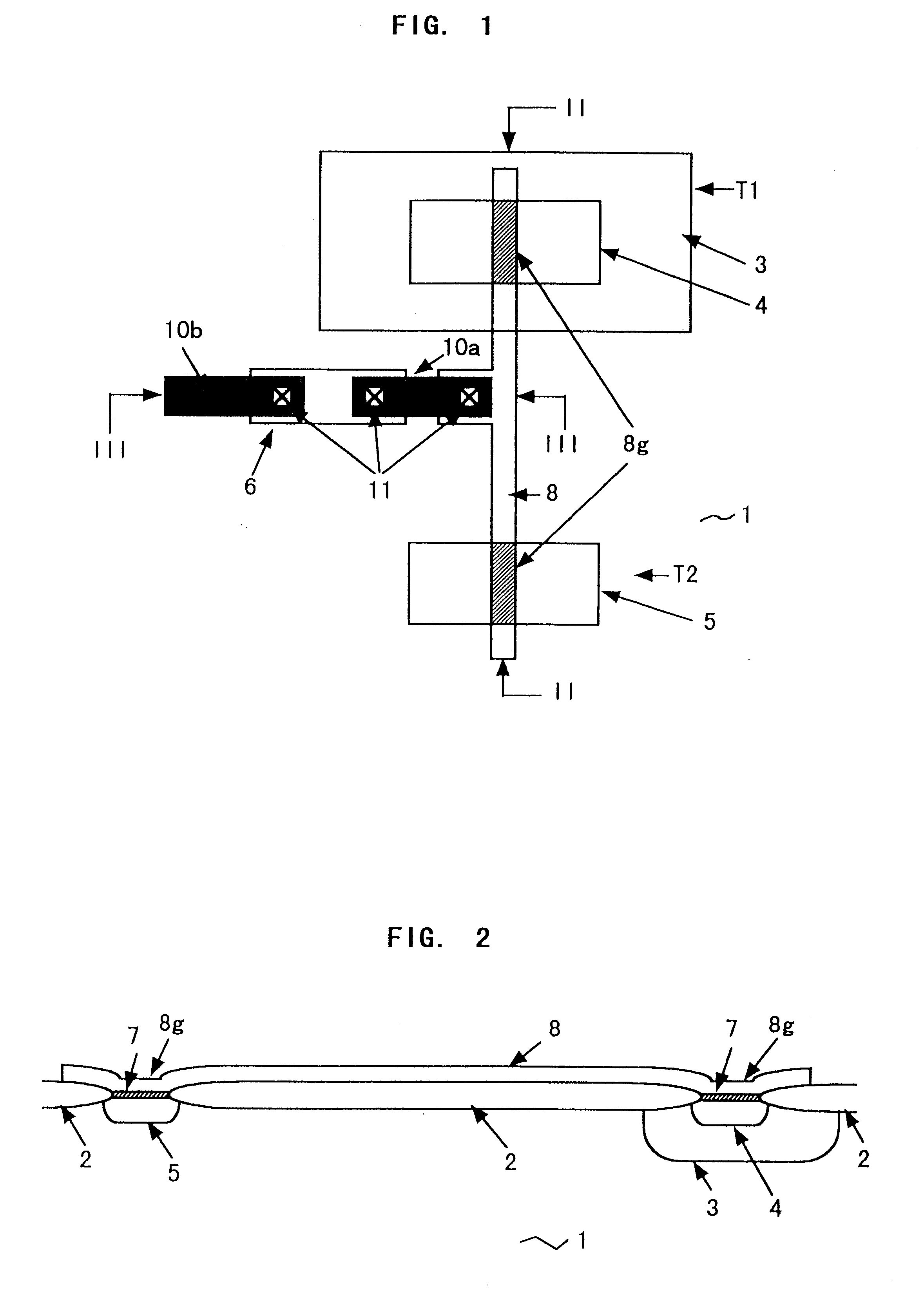
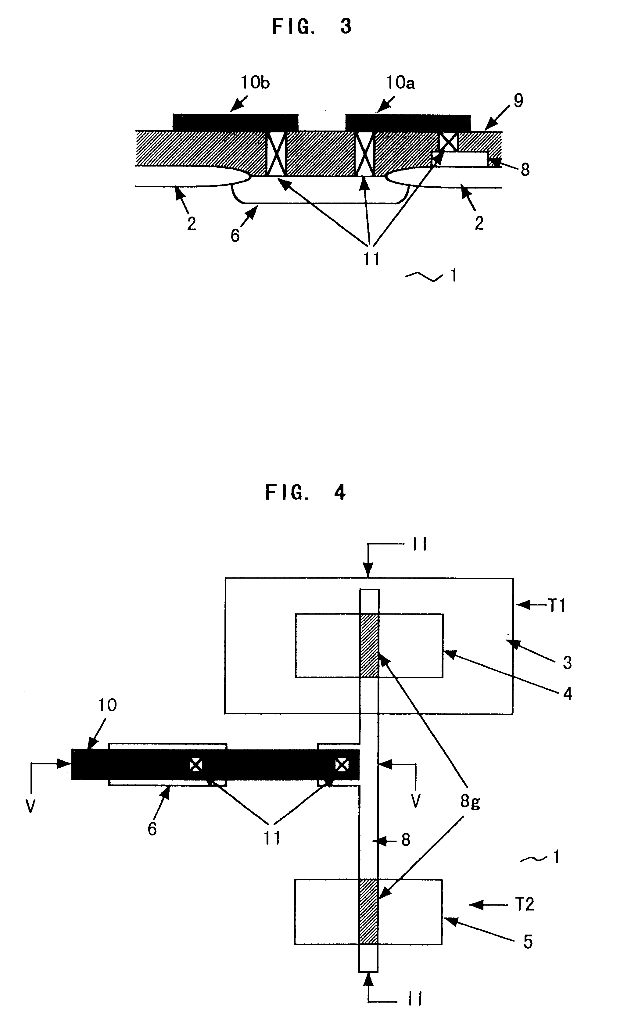
FIGS. 1, 2, and 3 are diagrams for illustrating a configuration of a semiconductor device according to a first embodiment of the present invention. FIG. 1 is a plan view showing a layout pattern of a standard cell, FIG. 2 is a sectional view taken on II--II line in FIG. 1, and FIG. 3 is a sectional view taken on III--III line in FIG. 1.

Referring to FIGS. 1 to 3, there are shown a p-type silicon semiconductor substrate 1 (hereinafter referred to as p-substrate, or substrate, when appropriate), an isolation oxide film 2 formed on a surface of the p-substrate 1, an n-type well 3 (hereinafter referred to as n-well, when appropriate) formed in the p-substrate 1, a p-type diffused region 4 formed in the n-well 3, an n-type diffused region 5 formed in the p-substrate 1, and another n-type diffused region 6 formed in the p-substrate 1.

Shown also in FIGS. 1 to 3 are a gate oxide film 7 formed on the p-type diffused region 4 and the n-type diffused region 5, a polysilicon wiring line 8, gate ...

second embodiment

FIGS. 4 and 5 shows the configuration of a semiconductor device according to a second embodiment of the present invention. FIG. 4 is a plan view showing a layout pattern of a standard cell, and FIG. 5 is a sectional view taken on V--V line in FIG. 4. A sectional view taken on II--II line in FIG. 4 is similar to the sectional view shown in FIG. 2.

Referring to FIGS. 4 and 5, a metal wiring line 10 works as an input line for the MOS transistor in the standard cell. In FIGS. 4 and 5, components like or corresponding to those shown in FIGS. 1 to 3 are designated by the same reference numerals, and the description thereof will be omitted to avoid duplication.

In this second embodiment, the metal wiring line 10 serving as an input terminal is not cut. However, a diffused region 6 is formed under the metal wiring line (or metal terminal) 10, and the metal wiring line 10 is connected through a contact hole 11 to the diffused region 6.

Although the junction of the diffused region 6 and the wafe...

third embodiment

FIGS. 6 and 7 shows a configuration of a semiconductor device according to a third embodiment of the present invention. FIG. 6 is a plan view showing a layout pattern of a standard cell, and FIG. 7 is a sectional view taken on VII--VII line in FIG. 6. A sectional view taken on II--II line in FIG. 6 is similar to the sectional view shown in FIG. 2.

Referring to FIGS. 6 and 7, a relatively large n-type well 3 is formed in p-substrate 1, and a p-type diffused region 12 is formed on the surface of the n-type well 3. In FIGS. 6 and 7, and in the succeeding figures, well contacts are not shown for simplicity.

In the third embodiment, a metal wiring line, which serves as an input line (input terminal), is divided into metal wiring lines 10a and 10b. The metal wiring line 10a is connected to gates 8g, and the metal wiring line 10b serves as a metal terminal. The metal wiring line 10a and 10b are connected by a p-type diffused region 12 formed on the surface of the n-type well 3. The resistanc...


PUM


Abstract

In a semiconductor device provided with a plurality of standard cells each comprising an input terminal and MOS transistors, a diffused region having a substantially negligibly small resistance is formed in a semiconductor substrate, and the input terminal of the standard cell and gates of the MOS transistors are connected through the diffused region. Also, a diffused region is formed under the input terminal in the substrate, and the input terminal is connected to the diffused region. In a modification, another standard cell is formed by forming a diffused region and a metal layer connected to the diffused region on the substrate, and the another standard cell is connected to the input terminal.

Description

1. Field of the InventionThe present invention relates to a semiconductor device provided with a library of standard cells which include MOS transistors and the gates of the MOS transistors have not undergone plasma damages. The present invention also relates to a method of designing such a semiconductor device.More specifically, the present invention relates to a structure of a semiconductor devise and a method of designing such a structure which prevents gates of MOS transistors from undergoing plasma damage in a wafer process in fabricating a semiconductor device.2. Background ArtFIG. 23 is a plan view showing a conventional standard cell layout pattern employed in auto-placement and auto-routing for a semiconductor device comprising a plurality of standard cells. Referring to FIG. 23, a standard cell has an n-type well 3 formed in a p-type silicon substrate 1. A p-type diffused region 4 is formed in the n-type well 3. An n-type diffused region 5 is formed in the p-type silicon s...

Claims


Application Information

Patent Timeline
Patent Type & Authority Patents(United States)
IPC IPC(8): H01L27/118H01L21/822H01L21/336H01L21/8234H01L27/04H01L27/06H01L29/78
CPCH01L27/11803
Inventor KANAMOTO, TOSHIKIAJIOKA, YOSHIHIDESHIMAZU, YUKIHIKOHAMADA, HIDEYUKI
Owner RENESAS ELECTRONICS CORP
Why Eureka
Try Eureka