Memory array organization and related test method particularly well suited for integrated circuits having write-once memory arrays

a write-once memory array and write-once technology, applied in the field of three-dimensional arrays, can solve the problems of inability to program memory cells, difficult test problems for manufacturers of write-once memory arrays, and inability to provide assurance against individual defects that may affect isolated memory cells or individual rows or columns of memory cells

Inactive Publication Date: 2003-02-04
SANDISK TECH LLC
View PDF11 Cites 52 Cited by
  • Summary
  • Abstract
  • Description
  • Claims
  • Application Information

AI Technical Summary

Problems solved by technology

Manufacturers of integrated circuits that include write-once memory arrays (also known as one-time programmable, or OTP memory arrays) face a difficult test problem.
The memory cells of the array must be assured of being successfully programmed by a subsequent user, but the manufacturer cannot program the memory cells during the testing procedures to confirm that each memory cell can be programmed, because the memory cells, once written, cannot be re-written or erased before shipping to an end user of the integrated circuit.
While such a structure may provide adequate general characterization of the memory cells formed nearby, it provides no assurance against individual defects that may affect isolated memory cells or individual rows or columns of memory cells.
Because of the inability to provide total assurance of a memory array, manufacturers sometimes warranty a device to be fully programmable for at least a specified percentage of the memory cells.

Method used


Image

  • Memory array organization and related test method particularly well suited for integrated circuits having write-once memory arrays
  • Memory array organization and related test method particularly well suited for integrated circuits having write-once memory arrays
  • Memory array organization and related test method particularly well suited for integrated circuits having write-once memory arrays

Examples


Embodiment Construction

)

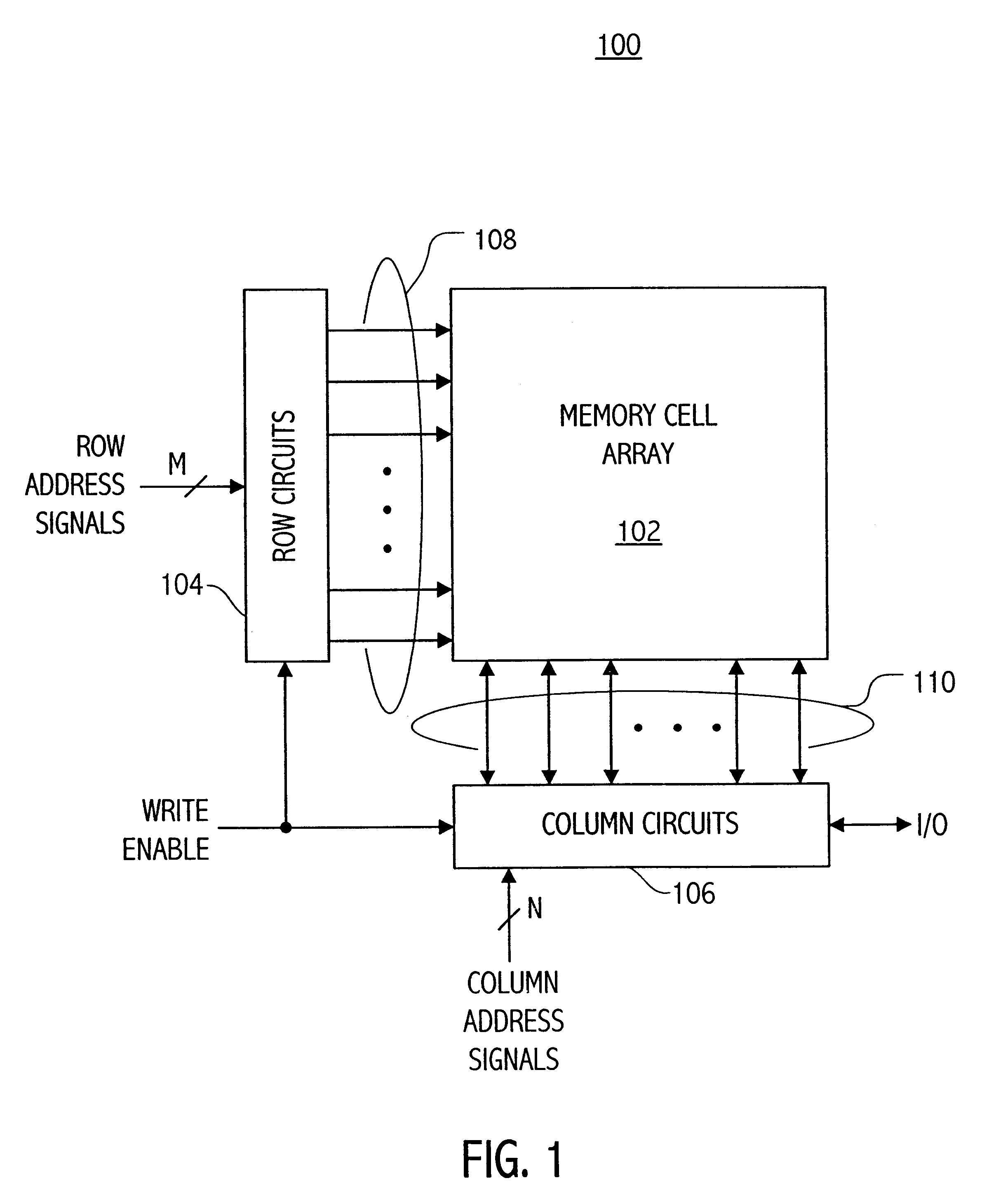
Referring now to FIG. 1, a block diagram is shown of an integrated circuit 100 including a memory array 102, which diagram may be useful to depict several preferred embodiments of the present invention. In one such embodiment, the memory array 102 is preferably a three-dimensional, field-programmable, non-volatile memory array having more than one level of memory cells, and which utilizes a read voltage different in magnitude from a write voltage. Preferred three-dimensional memory arrays are disclosed in commonly-assigned U.S. Pat. No. 6,034,882, entitled "vertically Stacked Field Programmable Nonvolatile Memory and Method of Fabrication," which patent is incorporated herein by reference in its entirety. Another preferred three-dimensional, field-programmable, non-volatile memory array technology is disclosed in co-pending, commonly-assigned U.S. patent application Ser. No. 09 / 560,626, entitled "Three-Dimensional Memory Array and Method of Fabrication," filed Apr. 28, 2000 and nam...


PUM


Abstract

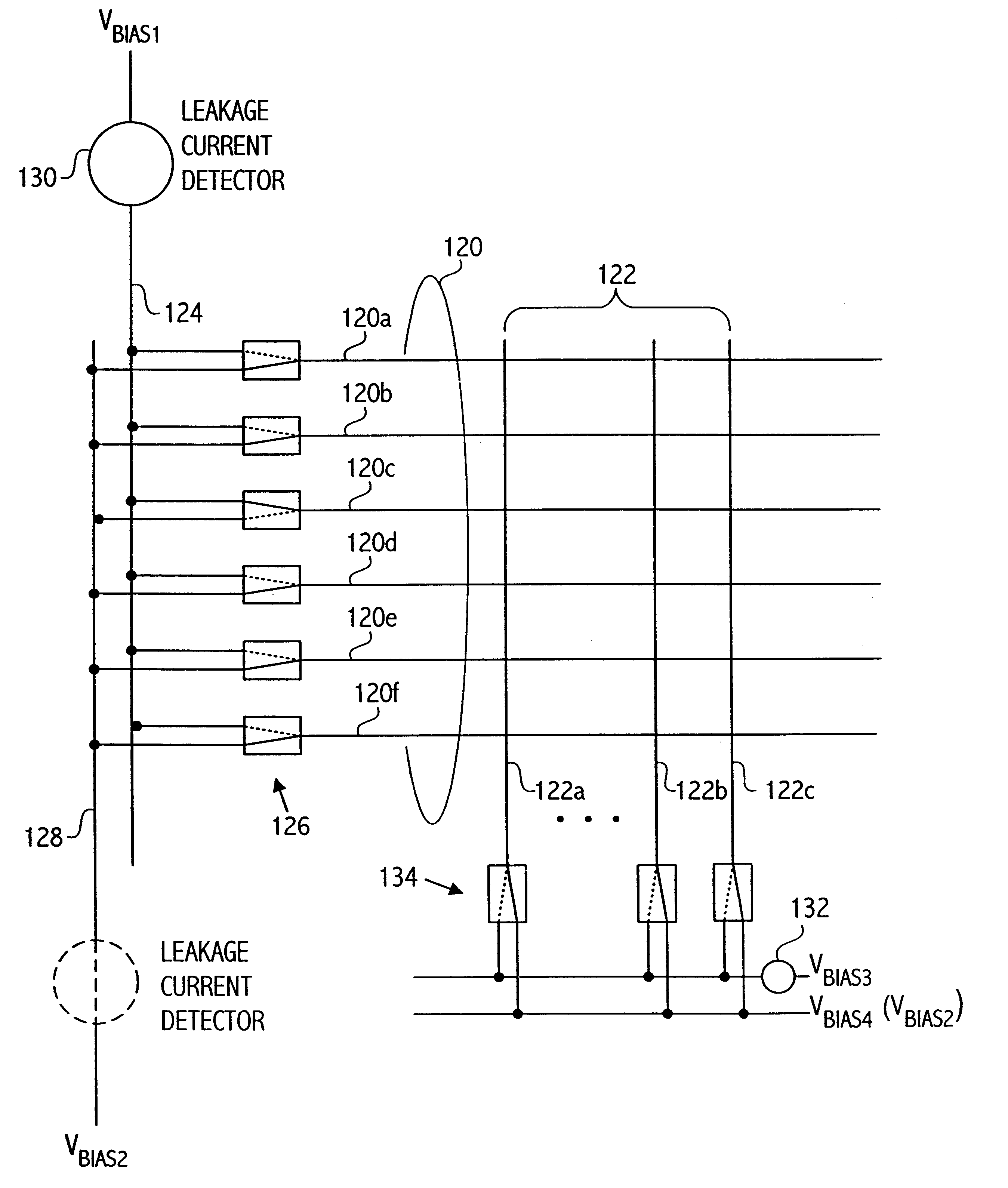
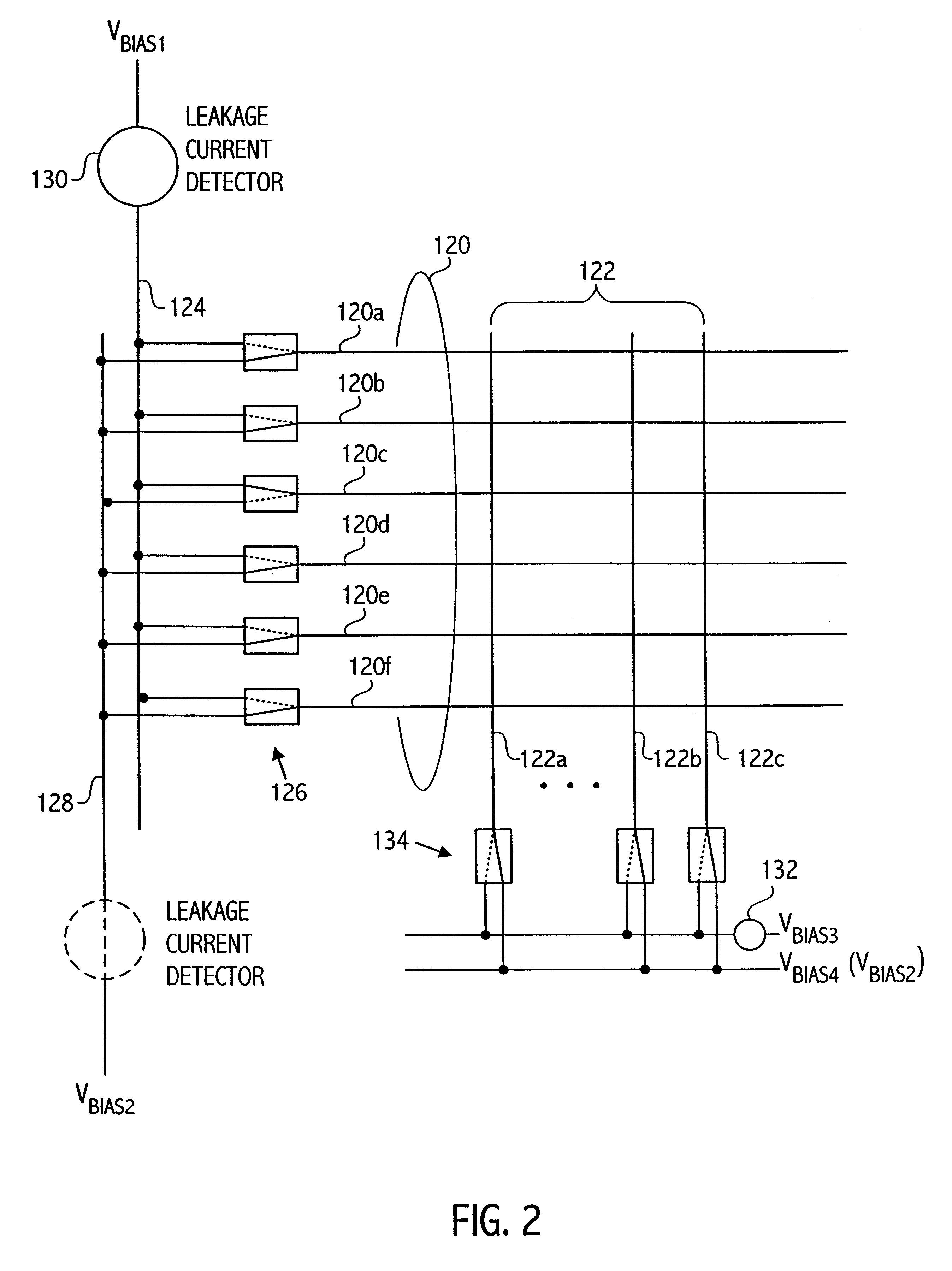
In a preferred integrated circuit embodiment, a write-once memory array includes at least one test bit line which provides a respective test memory cell at the far end of each respective word line relative to its word line driver, and further includes at least one test word line which provides a respective test memory cell at the far end of each respective bit line relative to its bit line driver. An intra-layer short between word lines may be detected, such as during manufacturing testing, by biasing adjacent word lines to different voltages and detecting whether any leakage current flowing from one to another exceeds that normally accounted for by the memory cells and other known circuits. Intra-layer bit line shorts and inter-layer word line and bit line shorts may also be similarly detected. An "open" in a word line or bit line may be detected by trying to program the test memory cell at the far end of each such word line or bit line. If successfully programmed, the continuity of each word line and bit line is assured, and the programming circuitry for each word line and bit line is also known to be functional.

Description

1. Field of the InventionThe present invention relates to semiconductor integrated circuits having memory cells arrays, and particularly to three-dimensional arrays incorporating multiple levels of memory cells.2. Description of the Related ArtManufacturers of integrated circuits that include write-once memory arrays (also known as one-time programmable, or OTP memory arrays) face a difficult test problem. The memory cells of the array must be assured of being successfully programmed by a subsequent user, but the manufacturer cannot program the memory cells during the testing procedures to confirm that each memory cell can be programmed, because the memory cells, once written, cannot be re-written or erased before shipping to an end user of the integrated circuit.Traditionally, several techniques have been utilized to increase the assurance level that a memory array, once shipped, will indeed be programmable by an end user. In one such technique, extra memory cells may be implemente...

Claims


Application Information

Patent Timeline
Patent Type & Authority Patents(United States)
IPC IPC(8): G11C29/24G11C29/04G11C29/02
CPCG11C29/24G11C29/02
Inventor CLEEVES, JAMES M.
Owner SANDISK TECH LLC
Why Eureka
Try Eureka